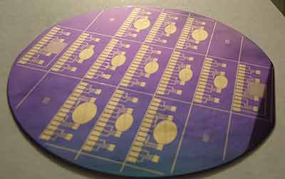
We use these as substrates to fabricate custom microelectrode arrays for in vitro electrophysiology. So we fabricate electrodes on these substrates and use those to record from cultured neurons or acute brain slices.
Substrates Used to Fabricate Microelectrode Arrays
Glass To Fabricate Microelecrode Arrays (MEAs)
A PhD research scientist used our soda lime glass for the microelectrode array experiments.
Get Your Quote FAST! Or, Buy Online and Start Researching Today!
Glass Substrates to Fabricate Microelectrode Arrays
An electrical engineer requested the following quote:
Would you be able to send me some information on the pricing of glass and quartz square wafers with 2” dimension with 0.5 and 1mm thickness. These are intended to be used for fabrication process of microelectrode arrays.
UniversityWafer, Inc. Quoted:
| Item # | Pol | Dia | Thick | Grade | Top side Ra | Backside Ra |
| U01-230228-5 | DSP | 50x50mm +/-0.2 | 0.5±0.025mm | JGS2 | < 1 nm | < 1 nm |
| U01-230228-6 | DSP | 50x50mm +/-0.2 | 1.0±0.025mm | JGS2 | < 1 nm | < 1 nm |
Reference #137367 for specs and pricing.
What Substrates are used to Fabricate Microelectrode Arrays?
I was wondering if you guys have the capability to grow a PECVD layer of Si3N4 (0.25um to 0.5um thick) on metallized wafers. We also have a cleanroom and can do almost our entire process except for this step. Currently, we have limitations where we can only grow Si3N4 in our PECVD on non-metallized wafers. I"m trying to make gold microelectrode arrays for a research project but having difficulty getting high quality nitride by sputter deposition.

I am seeing a lot of these types of gold micro-electrode arrays made with a Si3N4 dielectric (grown by PECVD) in the literature (mostly from Europe), but it seems no one allows metals in their PECVD here in the States. I saw from your website that you have similar restrictions but was hoping that you might have a separate PECVD or at least point me in the right direction for somewhere to do this here in the States.
This is for a research lab, and in all likelihood would only involve 5-10 4" wafers in total. The wafers consist of photolithographically patterned Au on SiO2 (with a Ni adhesion layer in between). I attached a picture to help explain.
Answer:
Yes, we can do PECVD Low Temp Low Stress Nitride on the Front Surface of these wafers. 5,000 angstroms +/-10% PECVD Low Temp Low Stress Nitride on up to 25 pieces of 100mm (std thickness) is a lot charge
Reference #187747 for specs and pricing.
What are Microelectrode Arrays (MEAs)?
Microelectrode arrays (MEAs) are commonly used in neuroscience and other fields to measure the electrical activity of cells, tissues, and organs. The choice of substrate for fabricating MEAs depends on several factors, including the specific application, the desired properties of the electrodes, and the fabrication process. Some common substrates used to fabricate MEAs include:
-
Silicon: Silicon is a common substrate for MEAs because of its high mechanical strength and electrical properties. It is also compatible with standard microfabrication processes, making it easy to integrate with other electronic components.
-
Glass: Glass is another common substrate for MEAs due to its transparency, which is useful for applications where visual access to the underlying tissue is required. It also has good electrical properties and is biocompatible.
-
Polyimide: Polyimide is a flexible polymer that can be used as a substrate for MEAs. It is commonly used for applications where the electrode needs to conform to the shape of the tissue or organ being measured.
-
Quartz: Quartz is a substrate that is often used for applications that require high stability and low noise. It is also transparent and has good electrical properties.
-
Titanium nitride (TiN): TiN is a conductive ceramic that can be used as a substrate for MEAs. It is biocompatible, corrosion-resistant, and has good electrical properties.
Other substrates used for MEAs include various polymers, metals, and ceramics, depending on the specific application and desired properties of the electrodes.
