What is a MOCVD Reactor?
MOCVD Service
Our MOCVD service can fabricate GaAs and InP substrates with superior quality and low cost. With our service, you can get the best performance from your devices while keeping your production costs low.
We have:
- in single or multi-wafer reactors
- on substrates 2", 3", 4" and 6" diameters
- all customized
Examples or recent order include:
2"Ø GaAs:Si/GaAs Epi wafers
Substrate: Gallium Arsenide wafers, P/P 2"Ø×325±25µm,
undoped GaAs:-[100]±0.5°,
Ro>1E7 Ohmcm, EPD<5,000/cm²,
Both-sides-polished,
Epi layer: 1.0±0.1µm, n-type GaAs:Si,
Nc=1E17/cc ±15%, grown by MOCVD,
Sealed under nitrogen in single wafer cassette.
Wafer: 2"Øwith InGaAs EPI on SI InP <100>, by MOCVD deposition
Substrate: Semi-Insulating InP (InP:Fe),
Resistivity: > 1 x 10E7 Ohm cm, EDP < 1 x 10E4/cm2)
EPI: Lattice matched In/Ga alloy layer of n-type InGaAs
Nc > 2 x 10E18/cc (using Si as dopant)
Thickness: 0.5 um (+20%)
Get Your MOCVD Quote FAST!
Metal-Organic Chemical Vapour Deposition (MOCVD) Tutorial
MOCVD-Metal Organic Chemical Vapor Deposition | Meaning, Explanation, Importance using Diagram |
What Are MOCVD Reactors?
During the growth process of metalorganic crystalline thin films, the ultrapure precursor  gas is introduced into the reaction chamber. A carrier gas is usually injected as well, which is nonreactive. The group III and V precursors can either be metalorganics or hydrides. Indium phosphide is grown using a trimethylindium or phosphine precursor. The resulting film is very thin and has a high-quality structure.
Metal-Organic Chemical Vapour Deposition (MOCVD) reactors have a number of advantages over conventional processes. For example, the MOCVD process is easy to scale up and is more flexible. The main advantage of this method is its ability to produce nanoparticles with higher density and purity than conventional methods. Furthermore, it has the advantage of being versatile and scalable. In this way, it can be used for both high-tech and low-tech industries.
The process of MOCVD has several drawbacks. Depending on the carbide stability, amorphous and graphitic carbon may be produced. This carbon is highly flammable and can also lead to the formation of a toxic gas. For this reason, the process is scalable and efficient. At the Cambridge Centre for Gallium Nitride, we have three commercial reactors. Its aim is to stimulate ideas and sensitize readers about this problem.
In addition to being inexpensive, MOCVD reactors can produce ultrathin film layers with higher uniformity. This process is very useful in the semiconductor industry and offers a cost-effective solution for the production of high-volume thin films. AMOCVD reactor's surface area increases, which means it can be used to make larger devices. AMOCVD can be scaled up to large scale for higher volume operations.
The MOCVD process has several disadvantages, and is limited by the availability of starting molecules. The technology has a low sensitivity to oxidation, which makes it a perfect candidate for MOCVD. It also has high sensitivity to temperature, making it ideal for use in applications where large-volume manufacturing is required. If you're in the early stages of the process, it's best to start with a simple test sample and experiment to determine its efficiency.
The MOCVD reactor is similar to a close-coupled showerhead. It consists of a chamber with gas inlets and gas outlets. Incoming gases transport group III metal organic precursors and group V gas hydrides. During the process, these precursor gases undergo chemical reactions. The chemical reactions in a MOCVD reactor are highly efficient and profitable. The high yield and low cost make the process a cost-effective alternative for manufacturing LEDs.
The MOCVD process is a multi-reaction chamber ring-shaped reactor. It is composed of sheet chambers and a cyclic center. The cyclic center is located in the preparation room. The ring-shaped chambers are used for chromium nitride and CoGa. The latter material is a highly effective and efficient LED. Despite the complexity of the process, the high yield is not the only advantage.
The basic design of MOCVD reactors is very similar to the hexagonal structure. Its multi-reaction chamber MOCVD drum contains seven chambers with different reactions. The reaction chambers are separated by a cyclic center. During the growth process, the materials are fused. Then, the catalysts are added to the liquids. When the polymerized substance is cured, the metal oxides are removed.
The multi-reaction chamber MOCVD reactor drum is composed of sheet chambers, which are arranged in a ring shape. The preparation room houses three MOCVD reactors. In the early 1980s, the AIXtron 200/4 was the first commercially available InP laser. Aixtron then launched the AIX 2000 Planetary Reactor series, which was used to produce red LEDs, space solar cells, and the first commercially available HBT.
The MOCVD process has many advantages over physical processes. Compared to the traditional processes, it is more flexible and easier to automate. In addition, the process also yields metastable materials. It is important to note that the MOCVD technology is the core technology of MicroLink. All of its staff are experts in the field and can help you make the best possible product. Its team possesses decades of experience in the field and is recognized internationally.
Metal Organic Chemical Vapor Deposition
Metal Organic Chemical Vapor Deposition (MOCVD) is a process used for creating highly  pure crystalline compounds with high atomic density. This method can also produce micro and nano structures. The key advantages of MOCVD are its ability to provide a highly controlled dopant concentration, precise fine tuning, and rapid synthesis. Hence, it is widely used in LED and laser diode manufacturing.
In MOCVD, the precursor gases are ultra-pure, so that they are suitable for the deposition of semiconductor films. They are injected into a reactor, along with a carrier gas, and are deposited on a heated substrate. The organic gas is then consumed due to pyrolysis on the surface of the substrate. Although it is a fast and reliable process, MOCVD is expensive, which makes it unsuitable for small laboratories.
The technique uses ultra-pure gases that are injected into a reactor. The precursor gas is usually a non-reactive gas, like nitrogen. The group III and V precursor gases are typically metalorganics. Indium phosphide, for example, can be grown using a hydride or trimethylindium precursor. The latter two are also common in the process of MOCVD.
MOCVD is a process in which a liquid metal organic precursor is deposited on a hot surface with the aid of a carrier gas. The process is typically conducted in a vacuum. This technology is used to deposit group III-V semiconductor devices. It is also a common technique for the production of silver oxide and other alloys. Because of the low cost and uniformity, it is a popular process in the manufacturing of optoelectronics and other semiconductors.
The process uses an ultrapure precursor gas that is injected into a reactor. The precursor gas is generally a non-reactive material that is injected into the reactor. The two types of materials are then deposited on the substrate. This process is also known as MOCVD. There are many different types of MOCVD. Indium and titanium oxide are the most popular materials deposited with this technique.
MOCVD is an epitaxial process that uses a pedestal as a susceptor. The material is heated in the reaction chamber. The precursor is deposited onto the substrate. The substrate is cooled after the process. After the reaction, the substrate is transferred to another chamber where it is exposed to the substrate. This is the simplest and fastest process in the industry. The precursor can be amorphous or crystalline.
MOCVD uses ultrapure precursor gases to deposit the metal on the substrate. The materials are deposited on the substrate by a high-temperature method, and the precursor gas is a non-reactive material. The process can be carried out in vacuum or in a semi-conductor process. It is often used for thin-film transistors and other high-tech applications. Aside from the fabrication of semiconductor devices, MOCVD is also used for research and development.
Compared to MBE, MOCVD provides a higher throughput for the metal-based substrate. It is also the process of choice for most compound semiconductor devices. It is a popular technique for producing thin-films. It is a process that requires very little preparation and enables manufacturers to achieve high quality results. It can also be used for manufacturing optoelectronic devices. But a cold-wall reactor is not ideal for this process.
MOCVD is a process that uses ultrapure metalorganics and hydrides as precursors. The process is more efficient than MBE because the substrate is not exposed to high temperatures and can be used more efficiently. For many applications, MOCVD is the most popular technique for semiconductor fabrication. The technology is a great tool for semiconductor industry and helps engineers make complex electronics. This type of semiconductor device is not only affordable, but it is also safe.
A high-temperature environment is essential to the process. The high temperature of the process is required to create the desired material. However, it can be a complex process. A reactor is a chamber that is designed to withstand high temperatures, and its walls are usually made of stainless steel or quartz. The walls of the reactor are lined with special glasses, which prevent the reaction from affecting the glass. The substrate is a flat, temperature-resistant material that sits on the top of the reactor.
What Are MOCVD Equipment?
If you're starting a new company or you want to start a small business, MOCVD equipment is a great place to start. This technology produces a variety of materials such as inorganic and organic semiconductors. It also helps you make the next generation of displays and electronic devices. For instance, microLEDs and miniLEDs are ideal candidates for next-generation displays. In addition, vertical-cavity surface-emitting lasers, or VCESLs, are being used to make facial recognition features on smartphones. These devices convert electrical energy into visible light and unlock the device.
After loading wafers into a MOCVD system, pure gases are introduced into the reactor. The gas flow contains chemical precursors that react with the device's surface and grow crystalline layers on the device. This method of crystallization is known as epitaxy, and is widely used for semiconductors and other III-V materials. Gallium nitride-based materials, including sapphire and silicon, are created using MOCVD.
Today, MOCVD systems are popular in the LED industry. They can grow epitaxial layers and films, which are the components of the LED semiconductor architecture. In the past few years, MOCVD equipment manufacturers have advanced the science and improved the efficiency of the process, resulting in higher component performance and higher production throughput. Aixtron and Veeco have long shared the lead in the MOCVD equipment market, but AMEC has overtaken them in recent years.
The first MOCVD equipment is a cold-wall reactor. The substrate is placed in a cold-wall reactor, which is supported by a pedestal. The pedestal serves as the susceptor, while the walls of the reactor are made of quartz, which is highly transparent to electromagnetic radiation. The materials in these devices are applied to a wide range of applications. They are used in the production of quantum well lasers, LEDs, and other semiconductor components.
The first MOCVD equipment in the market is called a cold-wall reactor. It is a special kind of reactor that supports the substrate and pedestal. This machine is able to load and remove epitaxial wafers in one step. The second MOCVD equipment is known as a hot-wall system. Both of these types of machines are important in the semiconductor industry. If you're looking for a high-quality process, you'll want to look for an OEM with a high quality product.
The MOCVD equipment market has experienced a mixed picture in recent years. While some vendors are able to maintain profits, the demand for MOCVD equipment is expected to grow at a slower pace. In 2020, the market will reach $445 million, up from $465 million in 2019. This technique was invented by North American Aviation in 1968. It is used to deposit III-V and GaN on substrates. In the long run, the MOCVD technology is an indispensable tool for any manufacturing operation.
In the last few years, the MOCVD equipment market has experienced a mixed picture. While MOCVD equipment vendors are hoping that the market will recover in 2020, it may take some time. In 2020, the market is predicted to reach $445 million. In 2019, it was at $465 million. For the most part, the MOCVD equipment market is used to create materials that are used in different applications. For example, this technology has been used for semiconductors, VCSELs, mini/microLEDs, power devices, and RF devices.
The market for MOCVD equipment has seen a mixed picture. While vendors expect a rebound in 2020, the market has been flat for the past several years. In 2020, the market is projected to reach $445 million, up from $465 million in 2019. Despite the slowdown, MOCVD equipment will remain an essential tool in manufacturing. Historically, this technology has been associated with LEDs for decades. In the past decade, it has now become a popular technology for smartphones, including the iPhone X.
While the market is still experiencing a mixed picture, the overall outlook for MOCVD equipment is positive. It is expected to grow to $445 million by 2020, from its current level of $465 million in 2019. Founded by North American Aviation in 1968, MOCVD was a breakthrough technology in aerospace. The first tools were home-built and used to deposit III-V materials on the surface of a substrate. As the technology continues to grow, more companies are becoming interested in it and looking to purchase it.
Epitaxial Growth of a Semiconductor Material Using Metal-Organic Chemical Vapor Deposition (MOCVD) Process
The epitaxial growth of a semiconductor material using metal-organic chemical vapor deposition is a very versatile and cost-effective process. The material is directly deposited onto a substrate and has a very high resistivity. It can also be grown on an epitaxial buffer layer. The method is particularly effective for producing thin films with a wide band gap, and it has the advantage of being faster and more reproducible than Silicon implantation.
In a MOCVD reactor, metal-organic chemicals are deposited onto the substrate by a gas  phase reaction. This process is an excellent option for the fabrication of LED chips, and it allows a thin, clean epitaxial layer. It has a relatively high rate of success, and the method has a wide range of applications. For example, the technology can be used to grow a variety of types of electronic devices.
The novel MOCVD reactor is illustrated in Fig. 1a and b. The MOCVD system features five independent gas inlets. Each of the precursor gases enters at its own independent entrance. This approach avoids pre-reactions and provides a very clean epitaxial layer. Moreover, a patented method enables the creation of highly efficient devices with a large number of features.
The epitaxial reactor is an important component of the CSBH laser fabrication process. It is used to grow crystalline semiconductor layers using the MOCVD process. The MOCVD epitaxial reactor is described in U.S. Pat. No. 4,716,130. It comprises a gas bed containing Fe and an S-doped InP layer. The n-type InP substrate is oriented in the (100) plane to produce the n-type epitaxial layer.
The MOCVD reactor has been successfully used for fabrication of CSBH lasers. The MOCVD process is a metal-organic chemical vapor deposition process and is similar to MOCVD. It uses a chemical solution called nitric acid as an initiator and a slurry of the precursor materials. The precursors used in the CSBH are n-type InP.
The BDS MOCVD reactor is a very efficient and effective process for epitaxial growth of semiconductor materials. The MOVDR process operates at moderate pressures. The resultant epitaxial layer is clean and uniform. The MOVDR reactor is an excellent choice for manufacturing devices and is an alternative to silicon. This process can be carried out at a very low cost and can yield a very large number of applications.
The n-type InP substrate is a semiconductor material with a P-type structure. In addition to InP, the Fe-doped P-type InP is an n-type semiconductor material with a P-type structure based on the n-type InP layer. The S-type epitaxial film is oriented in the n-type direction.
The n-type InP substrate is an n-type InP substrate with Fe-doping. The InP substrate was grown on an n-type InP substrate 22. It is a S-doped LEC material and oriented along the (100) plane. A n-type InP material with an S-type structure is the best epitaxial material.
The MOCVD method was used to create a CSBH laser with a large beam angle. The MOCVD method was used to grow Fe-doped InP on n-type InP substrate 22. The inert material was oriented in the (100) plane. The n-type InP substrate was placed on the surface of the n-type LEC.
The growth of a GaN-based layer on sapphire substrates was demonstrated using a MoCVD reactor. The film was deposited on the substrate and was then cooled. After the growth was completed, the InP-based layers were investigated for their optical properties. The GaN-based films are characterized by their high dimensionality. The synthesis of these devices requires a large amount of energy.
The MOCVD reactor is designed with a single inlet port. The gas supply system is used to supply multiple gases simultaneously. The first reactant gas is introduced into the chamber through the inlet 510. The second reactant is introduced into the chamber through tubing 530 and 540. The growth rate is dependent on the concentration of the reactants. The larger the total gas flow, the faster the reaction.
What is MOCVD Process?
The MOCVD process is a versatile technology for producing compound semiconductors. The method involves vaporization of a mixture of chemicals and transport of these gases into a reactor. The reaction results in the formation of a new epitaxial layer of the semiconductor crystal lattice. The use of high-quality MOCVD equipment enables a cost-effective production solution. The kSA ICE metrology tool is compact and offers direct substrate and wafer carrier temperature measurement, thin-film stress and curvature measurement, surface roughness and texture in real-time.
This method is commonly used to produce thin layers of atoms on a semiconductor wafer. 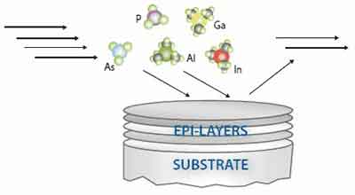 It is also known as metal organic vapor phase epitaxy or organometallic chemical vapor deposition. AIXTRON is a leading MOCVD tool manufacturer and has developed a unique platform to enable the production of compound semiconductor devices. You can use one of the AIXTRON tools to achieve a wide range of materials.
MOCVD uses ultrapure precursor gases to deposit a thin layer of atoms onto a semiconductor wafer. A non-reactive carrier gas is used to carry the precursors. The precursor gases include hydrides and metalorganics. The MOCVD process is also used to grow p-GaN-based semiconductors. The company AIXTRON also has two different MOCVD processes, Close Coupled Showerhead (r) technology and the Planetary Reactor.
The MOCVD method is a versatile technology for semiconductor multilayer structures. The process can be used to make solar cells, LEDs, and high-speed transistors. It is a process in which ultrapure precursor gases are injected into a reactor. Typically, a non-reactive carrier gas is used. The group III and group V precursors are metalorganics, such as dimethylindium sulfide, hydrides, and nitrous oxide.
The MOCVD process uses a non-reactive carrier gas in the reactor. The ultrapure precursor gases are injected into a reactor by using a closed-coupled showerhead or a planetary reactor. The first step is to inject the two gases. The second step is the cooling process. In the MOCVD, the precursors are vaporized into a high-purity solution.
During the MOCVD process, ultrapure precursor gases are injected into the reactor. A non-reactive carrier gas is used to heat the reactor. In the MOCVD process, these gases are injected with a non-reactive carrier gas. Often, the group III and group V precursors are metallic hydrides or metalorganics. Indium phosphide is deposited using a trimethylindium or phosphine catalyst.
The MOCVD process uses ultrapure precursor gases to grow the semiconductor material. A non-reactive carrier gas is injected into the reactor with the precursor gases. Then, the precursors are deposited onto the substrate using a sputtering or evaporating material. This process is also used to manufacture GaN-based semiconductors. The most popular commercial MOCVD tools are produced by Structured Materials, Taiyo Nippon-Sanso, Valence Process Equipment, Veeco Turbodisc, and Aixtron.
This process involves the deposition of thin layers of atoms on a semiconductor wafer. The process is an important part of the manufacturing of GaN-based and III-V semiconductors. Several different kinds of catalysts can be used in the MOCVD process. A carrier gas is a carrier gas for the hydrogen-based precursors. Indium phosphide is grown by mixing indium hydride with a p-methylindium precursor.
This process utilizes a cold-wall reactor, which is designed to support the substrate. The substrate itself is supported on a pedestal that serves as a susceptor. The pedestal is the primary source of heat energy in the reaction chamber. Quartz walls are typically transparent to electromagnetic radiation, which is why this process is effective for creating high-purity crystalline compounds. AMOCVD is an efficient and versatile technology.
The process involves heating a hot-wall CVD chamber. This chamber is used to introduce gas through bubbles, which are a common part of the process. The metalorganic liquid is injected by a carrier gas. The carrier gas picks up the metalorganic vapour. The amount of metalorganic vapour transported depends on the bubbler's temperature. The nozzle's speed is also controlled.
What is MBE and MOCVD?
What is the difference between MBE and MOCVD? Both technologies utilize a gas or solid source to deposit materials. In MBE, gases have a relatively low pressure, typically around one x 10-4 mbar. They have longer mean free paths and are deposited on a substrate by diffusion. The atomic and molecular beams are generated by a solid source, while gas sources in CBE are vapors at room temperature.
| Feature | MBE | MOCVD |
| Source Materials | Elemental | Gas-Liquid |
| Evaporation | Thermal, e-beam | Vapor Pressure, Carrier Gas |
| Flux Control | Cell Temperature | Mass Flow Controller |
| Switching | Mechanical Shutters | Valves |
| Environment | UHV | H2-N2 (10-1000mbar) |
| Molecular Transport | Ballistic (mol. Beams) | Diffusive |
| Surface Reactions | Physi-Chemisorbtion | Chemical Reaction |
While both processes are effective for growing materials, they have different advantages. MBE allows the growth of large structures such as nanometer-sized polymers, while MOCVD is best for thin films and nanometer-scale materials. The atomic nitrogen and gas source in MBE is more stable than in MOCVD. MBE also limits the precipitation of metal droplets, which can result in large surfaces. The result is a layered InGaN/GaN structure.
MBE is more controlled and pure than MOCVD, and is more expensive. The gas source is easier to control and the growth rate is faster. The process is more suitable for low-volume production and R&D. Most MBE growth yields high-quality thin films. The difference between the two methods is mainly the method of selecting atoms or molecules to grow. The process also has a lower temperature range than MOCVD.
Both processes are effective for growing high-quality thin films. However, they are not the same. While CBE grows more quickly than MBE, CBE produces more pure and controlled films. This makes it more effective for manufacturing high-volume parts. Both technologies are capable of creating complex devices. They are also better for high-volume R&D than MBE. It is important to choose the best method for your needs.
While both techniques are effective in semiconductor manufacturing, MBE is less efficient than MOCVD. The difference between the two methods lies in the origin of the gas used. In MBE, the gas source is the same as in CBE. The gas source is a source of hydrogen. In CBE, the gas phase reacts with the material. In MBE, it is the other way around. MBE is better than MOCVD.
MBE and MOCVD are two common methods for deposition of thin films. MBE is the most pure form of the two, and is the most popular method for high-volume production. Its high-purity nature makes it ideal for high-volume MBE. Both methods can be used in the same applications. They can be adapted to meet the specific needs of the consumer. The best MBE is the one that works with the materials you need.
Both MBE and MOCVD are important techniques in semiconductor manufacturing. MBE is the better method. It can be used for semiconductor growth, while MOCVD is better for metals. MBE is more selective. It can also be used for more complex materials. In addition, both methods are characterized by high-purity growth. You can choose the process that works best for you. There are many differences between MBE and MOCVD.
Both techniques are used to grow thin films. InGaN is a better choice for semiconductor production. Its higher purity results in a layered structure of the material. But what is the difference between MBE and MOCVD? The difference between the two methods is the atomic nitrogen that is used. The two methods use the same plasma source, but the gas source is more powerful. While MBE is better for manufacturing, MOCVD has more advantages.
MBE is better for manufacturing thin films because it produces more atomically dense layers. InMBE, the nitrogen layer is made of inorganic materials. The InGaN layer has a high equilibrium vapor pressure, while the MBE layer is made of inorganic materials. Both technologies have a wide range of uses. MBE is used to grow films. InGaN is a crystalline material.
In MBE, the process uses a Rf plasma source to generate active nitrogen species. It uses pre-nucleated GaN/SiC substrates. The GaN layer was grown using MBE at 750-900degC and the InGaN layer was grown using the modulated beam technique. Unlike MOCVD, MBE is more powerful and has improved stability and efficiency.