We need the followng photoresist sensitive to 405nm UV light coated on one side.
300mm Silicon (100) <1ohm-cm 500-1000um
A university researcher requested the following quote:
We need the followng photoresist sensitive to 405nm UV light coated on one side.
300mm Silicon (100) <1ohm-cm 500-1000um
Reference #152171 for specs and quantity.
A postdoc requested help with the following:
We require a quotation for 25 “Borofloat 33” double sided polished [100mm diameter] with flat ,coated with 200nm of LPCVD polysilicon on both wafer faces. The Polysilicon coating has be done by LPCVD as this coating will be the mask for the wet etching of the Pyrex.
The thin polysilicon on the BF33 is patterned normally used photolithography. The exposed polysilicon is wet etched to gain access to the BF33. Photoresist is stripped. BF33 is then patterned using HF etch and using Polysilicon as the etch mask.
Get Your Quote FAST! Or, Buy Online and Start Researching Today!
An electrical engineering graduate student asked the folllowing question.
Since the oxide will grow on both sides, I expect you'll just remove the back oxide by covering the front with a photoresist, followed by an HF bath - correct? If so, what photoresist will you use? Our process is quite sensitive to ion contamination.
Answer: We use AZ-4620.
Reference #150667 for specs and pricing.
The technology behind photoresist is quite fascinating, but there are many ways to use it, and it can be hard to understand what each one does.
Photoresist is a light-sensitive material used in several processes, including photolithography, photoengraving, and photoresist etching. Each of these processes has its own unique benefits and purposes.
By understanding the basics of photoresist technology, you can better understand how it can be used in your industry. Our team at photoresist understands this technology inside and out, so we're here to help you every step of the way.
A medical student requested confirmation that the following specs would work for their project.
I would like to order some wafers for spin-coating photoresist and I am hoping you can help me pick the right kind. Basically I'd like to get the same kind that our microfluidics guru, usually gets. Here are some details he sent to me:
Item #452 - 100mm P(100) 0-100 ohm-cm SSP 500um Test Grade
Reference #126202 for specs and pricing.
A PhD candidate's research group requested a quote for the following:
Our university lab uses silicon wafers as a smooth substrate for deposition of a robust photoresist that becomes a raised pattern, acting as a sort of “stamp” for PDMS poured over the patterned wafer later on. We are therefore not concerned with the conductivity of the silicon, only that it is quite smooth and flat, and fairly inexpensive. I’m afraid I am not very familiar with the grading and descriptions of your Si wafer offerings, and I would appreciate your advice on selecting an appropriate material. Is the 4" P(100) 0-100 ohm-cm SSP 500um Test wafer just as smooth as any of the other 4” wafers? What would be the per-wafer cost if we only wished to order 5 wafers?
Reference #114299 for specs and pricing.
An optoelectronics researcher requested the following:
How are they packaged? I would be happy for them to be coated in photoresist, diced and then left on the backing sheet, unwashed for transport.
Reference #116620 for specs and pricing.
A Ph.D. Candidate of a Biomaterials & Biomedical Engineering department requested help with the following:
I'm currently designing a microdevice which requires me to use 25-50um wafers. I noticed that UniversityWafer supplied them, and I had a few questions about the wafers:
In terms of diameter, either 2" or 3" wafers should be fine, and I'd prefer it if the wafers were not doped. This isn't a hard requirement though, so it would depend on price. Would it be possible to get a ballpark estimate for the costs of:
In terms of handling, how do you package and ship them to prevent breakage? I'm trying to get a sense for what we can put them through and how many we will destroy before getting a working piece.
Reference #103099 for specs and pricing.
A scientist requested the following:
If I send you a 4in quartz wafer thick:625 um with patterns on one side, then can you thin down the substrate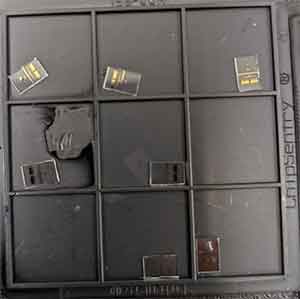 from the backside to about 50 um (or less) and also dice it to ~3mmx8mm? Please let me know the limitations of the thinning process so that we can adapt our design accordingly. If this is possible then please send me a quote. I can send you a box with 9 samples (image of a dummy box attached). Each sample is a 3.5mmx 7mm x 625um quartz substrate. There are Ti/Cr/Au patterns on the top. We want to preserve the Au pattern and thin down the substrate to 50um thickness. We can spin some photoresist on top to protect the surface."
UniversityWafer, Inc. Quoted:
We do on a best effort basis and please spin some photoresist on top to protect the surface first then yuo could send them to us to do sample try.
Please reference #266573 for pricing.
A photoresist is a light-sensitive material used in several processes, including photolithography, photoengraving, and photoresist etching. The main purpose of photoresist is to create patterned coatings on a surface. This process is extremely important in the electronics industry. The technology behind photoresist is quite fascinating, and there are many ways to use it. Here are three ways.
The first type of photoresist is called liftoff. This process applies thin films onto substrates using a cleanroom  environment. Liftoff takes place before deposition and chemical etch. A stepper is used to project circuit images onto a substrate. The light is projected through a mask to create a negative image. The second process, image reversal, reverses the tones of positive photoresists to reveal the underlying pattern.
Another type of photoresist is called liquid photoresist. A dry film photoresist is known as a dry film resist. It is used in semiconductors, plasma displays, and printed circuit boards. A liquid photoresist is more flexible than a standard film and is a better choice for sensitive applications. It is a versatile material that can be used in many applications, including semiconductors and LCDs.
Photoresist comes in different varieties, based on the application for which it will be used. Some types are made from liquid photoresist, while others are made of a thin film. The former is used in semiconductors, plasma displays, and printed circuit boards, while a dry film photoresist is used in electronics. It is also a common material in laser printing, as it helps in reducing the amount of light that will pass through the substrate.
The most common form of photoresist is the positive kind. It is sensitive to UV light and changes its chemical structure. The exposed areas of photoresist are soluble, while those not exposed to UV light remain insoluble. The negative type is used for the semiconductor manufacturing industry. It is a type of acetate that allows the fabrication of complex parts. The underlying material is made of silicon. In addition to semiconductors, it is also used for other applications.
There are two types of photoresist: dry and liquid. The latter is a thin film that resists exposure to UV light. The liquid form is used in semiconductors, while the dry film is used in plasma displays and printed circuit boards. This type is also used in the production of electronic devices. In other words, both types of photoresist are important. So, what is photoresist? There are many different uses for this chemical.
The main function of photoresist is to make it compatible with light-sensitive surfaces. Various types of photoresist are available in the market. The most common one is for forming printed circuit boards. It is essential for microprocessing, semiconductors, and flat panel displays. The image of the red arrow is made on the black part of the photoresist. In contrast, the dark color of the photoresist is visible only in ultraviolet light.
The positive photoresist is a material that is light-sensitive. Its use is limited by the number of possible substrates. The light-sensitive material is typically applied to the surface of a photoresist. In order to create a photograph, the photoresist must be suitable for the desired substrate. It must also be compatible with the printer. However, it must be able to print a high-quality image.
The sensitivity of photoresists depends on its sensitivity. It is a substance that will allow the exposed area to be revealed. During the process, it is crucial to use the UV-light-sensitive material as it can produce a high-quality image. This is important because it can be sensitive to UV light, which means that it is a type of UV-resistant material. In fact, the only way to determine if your photoresists are good enough to work is to check their quality.
The photoresists used in semiconductors are very light-sensitive polymers that change their structure when exposed to radiation. They are spun on a surface that is suitable for the exposure. After this, they are exposed to the radiation and can form thin layers. As a result, a high-quality photoresist can help in a variety of semiconductor processing processes. The following steps will be used in the manufacturing of photoresists.
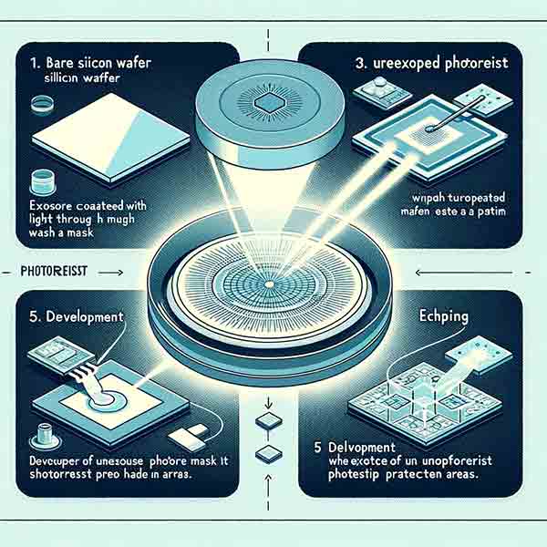
The use of photoresist in semiconductor manufacturing typically involves the following steps:
Cleaning: The silicon wafer is thoroughly cleaned to remove any contaminants that could affect the photoresist's adherence and the quality of the lithography process.
Photoresist Application: A layer of photoresist, a light-sensitive polymer, is applied to the surface of the silicon wafer. This can be done through techniques such as spin coating, where the wafer is spun at high speeds to evenly distribute the photoresist.
Pre-bake (Soft Bake): The wafer with the photoresist is baked at a moderate temperature. This step is crucial to remove the solvent from the photoresist and to harden the photoresist film slightly, making it more stable for the subsequent steps.
Exposure: The photoresist-coated wafer is then exposed to light (usually ultraviolet) through a photomask, which contains the desired pattern. The areas of the photoresist that are exposed to light undergo chemical changes.
Post-exposure Bake: This step involves heating the wafer after exposure to further induce the chemical reactions in the photoresist.
Development: The wafer is then developed in a solution that selectively removes the areas of the photoresist that have become soluble (in the case of positive photoresist) or leaves the insoluble areas (in the case of negative photoresist), revealing the underlying silicon wafer in the desired pattern.
Etching: Using the patterned photoresist as a mask, the exposed areas of the silicon wafer are etched away by chemical or plasma etchants.
Photoresist Removal (Strip): After the etching process, the remaining photoresist is removed from the wafer. This can be done using chemical solvents or plasma ashing.
Post-etch Bake: This optional step can be employed to harden the remaining features on the wafer and improve their resistance to subsequent processing steps.
Each of these steps is critical to the overall lithography process in semiconductor fabrication, allowing for the precise patterning necessary for integrated circuits.
What is inverse lithography and what can it bring to semiconductor manufacturing? Let's start with a brief overview of lithography, which we'll discuss in more detail in a moment. Photoresist and substrates are both used in semiconductor manufacturing. In this article, we'll talk about how photoresist and substrates can be used in inverse lithography.
Inverse lithography is a process for creating patterns on silicon chips by starting with the desired features on a wafer. Then, using computer algorithms, a photomask is designed to produce these features. Until recently, this process was impractical and too time-consuming for advanced chipmakers. But with the new technology, that's changing. ILT now provides a solution to the problem of a small, imperfect mask.
Inverse lithography is based on Level Set Methods, which are unified with the inversion process. The technique is used to insert SRAFs where they are needed without affecting the target pattern or the main pattern. This allows semiconductor companies to print more complex and more advanced chips without needing to upgrade their equipment. The resulting image may contain an infinite number of identical resist contours.
Inverse lithography technology (ILT) has the potential to dramatically speed up the process of making semiconductor chips. This new technique begins with the desired features on a wafer and computes the exact shape of the photomask needed to achieve those features. The conventional, lithographic method of creating chip layouts has proved too time-consuming for advanced chipmakers. However, the new method can reduce the time needed to perform this critical step to just one day.
Currently, IC design is still done with 193nm wavelength lithography. However, new techniques have been developed to mitigate the process variations caused by this new technology. In particular, lithography gap, which causes severe distortions due to optical diffraction, is a serious detriment to manufacturing yield. Hence, a complete paradigm shift in layout design is needed. But, how can it be implemented?
Inverse lithography (IL) technology can help push the limits of lithography while improving resolution and repeatability. Traditional ILT methods are time-consuming and inaccurate, but the new parallel, seamless-merging-oriented method is quick, accurate, and can take into account the environment. This is especially important for high-volume production in the semiconductor industry. The method is also ideal for complex device designs where the size and complexity of individual layers must be optimized.
Inverse lithography technology works by applying a plasma-based surface treatment. This process works by ensuring the wafer stage and reticle stages move continuously in sync during wafer exposure. One company, Canon, has developed a synchronization control technology that enables it to achieve sub-nanometer positioning accuracy. It uses a high-rigidity, lightweight stage to repeatedly accelerate the reticle stage at a rate of 12 G, resulting in high productivity.
The present invention relates to a multi-layer anti-reflective coating for semiconductor manufacturing photoresist. As technology continues to progress, semiconductor manufacturers are increasingly looking to new ways to minimize standing waves in photoresist. Moore's Law states that the number of transistors and other electronic devices per unit area doubles every 18-24 months. This rapid growth is the result of design improvements, including decreasing minimum feature sizes. Nowadays, the smallest semiconductor devices are 0.15 microns or smaller.
In inverse lithography, the photoresist layer 120 contains a thin layer of the semiconductor material. This layer has a high-intensity anti-reflective coating that helps reduce reflections. This new type of coating is used in the fabrication of high-quality devices. However, it is important to note that photoresist layers are difficult to remove once they have dried.
In a process similar to lithography, a thin layer of a photoresist material is spun onto a wafer, and the process moves from there to the underlying film using 193i PL tools. The key to this process lies in its ability to generate near-zero waste, since only a fraction of the volume of photoresist is used. The high-quality, low-volume process is an appealing option for semiconductor makers, and it will ultimately benefit existing semiconductor manufacturing companies and suppliers.
Inverse lithography is one of the most promising technologies for resolution enhancement, as it can push lithography to its limits. Existing ILT methods are time-consuming and inaccurate, but the new seamless-merging-oriented parallel method is fast and accurate, and takes environmental change into account. This technology has the potential to revolutionize semiconductor manufacturing. But it is a challenge to overcome. Here are some of the challenges of implementing the technology:
Video: Inverse Lithography Technology