Silicon Resistivity Ranges
What Silicon Resistivity Ranges Are Available?
The resistivity ranges for silicon wafers can be broadly categorized based on the type of doping and the intended application. Here's a general overview of resistivity ranges for silicon wafers:
Intrinsic (Undoped) Silicon
- High Resistivity: Typically > 1,000 ohm-cm, can go up to 10,000 ohm-cm or higher. This is common in applications requiring minimal electrical conductivity without the influence of added dopants.
Doped Silicon
N-Type (Doped with elements like Phosphorus, Arsenic)
- Low Resistivity: 0.001 - 0.005 ohm-cm for heavily doped wafers, used in applications requiring high electrical conductivity.
- Medium Resistivity: 0.005 - 10 ohm-cm, used for various electronics and semiconductor devices.
- High Resistivity: 10 - 100 ohm-cm or more, used in applications where moderate conductivity is needed.
P-Type (Doped with elements like Boron)
- Low Resistivity: Similar to N-type, 0.001 - 0.005 ohm-cm for heavily doped wafers.
- Medium Resistivity: 0.005 - 10 ohm-cm, suitable for a wide range of electronic applications.
- High Resistivity: 10 - 100 ohm-cm, for specific applications requiring controlled conductivity.
Special Applications
- Ultra-High Resistivity Silicon: > 10,000 ohm-cm, used in specialized applications such as high-performance radio frequency (RF) and microwave components, and in detectors for particle physics and astrophysics where minimal electronic noise is critical.
These ranges are indicative and can vary based on the manufacturer and specific requirements. Silicon wafer manufacturers often customize the doping level to achieve the desired resistivity for a particular research or industrial application.
UniversityWafer, Inc. inventory includes wafers that are <1 ohm-cm to greater than 20,000 ohm-cm in stock.
Get Your Quote FAST! Or, Buy Online and Start Researching Today!
What Silicon Wafer Resistivity is Available to Researchers?
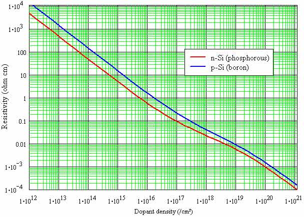
Silicon wafer resistivity available to researchers can vary widely, depending on the specific requirements of their projects. Generally, silicon wafers come in a range of resistivities to cater to different applications, from very low-doped (high resistivity) to highly doped (low resistivity) types.
For intrinsic (undoped) silicon, the resistivity is typically in the range of 1,000 to 10,000 ohm-cm. Doped silicon wafers can have resistivities as low as 0.001 ohm-cm for heavily doped n-type or p-type silicon, up to several thousand ohm-cm for lightly doped materials. The specific resistivity needed for a project depends on the intended application, such as microelectronics, photovoltaics, or MEMS (MicroElectroMechanical Systems).
Manufacturers and suppliers of silicon wafers can provide wafers with specific resistivity values according to the needs of researchers. To hit those precise resistivity numbers, manufacturers tweak the doping process with precision. This is key for researchers who need their silicon wafers dialed in just right for cutting-edge experiments. It's a bit like adding just enough spice to perfect a recipe—except here, it’s all about getting that semiconductor to behave exactly as planned. So when scientists ask for something specific, these suppliers are on it, mixing and measuring until they've nailed the custom spec down pat. You can also ask for custom resistivity levels if you're diving into some niche research. Say you've got a project that's off the beaten path, and standard options won't cut it. That's when tailored solutions come in handy. They tweak the doping during production to get you just what you need for your experiments—precision matters here, so don't hesitate to specify what you're after. This kind of attention to detail could be the difference between a breakthrough and a dead end in your work.
What Is Silicon Resistivity?
Basically, the resistivity of silicon wafers is defined as the property by which silicon is able to conduct electricity. Although it is not a property that can be directly measured, a good estimate can be obtained by using the following equation: r = 2 x h where is the resistance, h is the density of silicon, and x is the thickness of the silicon wafer.
What is Doping Density?
Basically, doping density is the number of atoms or ions of an element distributed within a given volume of glass. Doping is the deliberate introduction of impurities into the semiconductor, usually via ion implantation and post-annealing processing. The process is controlled by the acceleration voltage of the source ion beam.
Doping density refers to the concentration of dopants, or impurities, in a semiconductor material. Dopants are introduced into a semiconductor in order to alter its electrical properties. For example, if a semiconductor is doped with a small amount of phosphorus, it becomes an n-type semiconductor, which means that it has an excess of electrons. On the other hand, if a semiconductor is doped with boron, it becomes a p-type semiconductor, which means that it has a deficiency of electrons. The doping density is typically expressed in units of atoms per cubic centimeter.
Calculator
Getting an electrical resistivity calculator is useful when you are figuring out the resistance of a wire at different temperatures. The calculator is easy to use and will tell you exactly what you need to know. It is important to note that the resistivity of different materials will vary depending on the purity and the chemical makeup of the metal. There are also differences in the way the metals are manufactured.
In the world of electrical engineering, high-resistance substances are essential to a variety of applications. For example, silicon plays a vital role in transistor technology. This is due to its mobility. To calculate the resistance of a sheet of silicon, you will need to multiply the resistance by the thickness of the material.
A four point probe is an effective tool for determining the electrical resistance of a conductor. The four point probe uses the voltage across the two electrodes of a theoretical square to measure the resistance of a thin layer of material. A similar technique is used to calculate the conductivity of a thick layer.
There are a few different methods of calculating the resistivity of a sheet of material. One method is the ohms-per-square. This method uses a meter cube to determine the resistance of a layer of semi-conductive material. In a similar fashion, the ohms-cm is a method for measuring the bulk resistivity of a material.
The ohms-Centimeter is a unit of measurement of the volume resistivity of a material. The ohms-Centimeter can be used with a four point probe or with a meter cube. The ohms-centimeter is not limited to a meter cube, but it is best suited for measuring a single homogeneous material. The ohms-centimeter can also be used for measuring the volume resistivity of a three-dimensional material. It is also not as accurate as a meter cube, but it can be used to compare with other methods of calculating the volume resistivity of a material.
The electrical resistance of a conductor decreases with the increase in temperature. A carbon resistor has a resistance of -4.8 x 10⁻⁴ at 20 degC, but it drops to -4.8 x 10⁻³ at 120 degC. This is because of the way the metal is made. A similar effect is seen in alloys. The higher the purity of the alloy, the higher the resistivity of the alloy. The table below shows the resistivity of various metals based on their corresponding temperatures. The values are derived from a 20 degS reference. This table is a great place to start, but your calculations may need to be adjusted to fit your application.
The MDC Doping - Resistivity Calculator is a useful tool for converting doping to resistivity. This calculator will determine the theoretical bulk breakdown voltage of a material, based on the doping level. This calculation is done using ASTM formulae for resistivity.
Mechanisms governing electrical conductivity
Various mechanisms govern the electrical conductivity of silicon thin films. These mechanisms are based on the electronic structure of the material. Understanding the fundamentals of electrical conductivity is important for researchers of conductive materials. Using these fundamentals, the conductivity of a particular material can be easily evaluated.
The most basic of these mechanisms is the transfer of thermal energy from a source to a medium. This is a very important mechanism in many technological applications. For example, a USB drink cooler needs a high degree of thermal conductivity. It is also necessary for space travel. lightning is another example of a thermally conductive form of energy transfer. In addition, it is important for the operation of jet turbines.
Another important mechanism is the interaction of electrons. When a valence electron enters a conduction band, a hole is created apart. This creates the potential gradient, or Ohm's law. Increasing the energy of the valence band will increase the conduction band. In nonmetals, the valence band is composed of lower energy bonding orbitals.
The Drude model, which is a simplistic theory of conduction, predicts the conductivity of monovalent metals. The model uses classical mechanics to simulate the movement of electrons in a solid. The model is very simple and gives a reasonably accurate approximation of the conductivity of these materials. The model is not very useful in non-metallic conductors, however.
In crystalline materials, phonons are thermal vibrations that scatter electrons. The resulting scattering leads to a reduction in the conductivity of the material. A similar process occurs in semiconductors and ceramics. The higher the temperature, the lower the phonon conductivity. Nevertheless, the rthermal method is still valuable for understanding how the phonons move through a solid.
Besides the rthermal model, there are other models that are useful for understanding how the electrons move in a solid. These include the Ohmic and Poole-Frenkel conduction mechanisms. Each of these conduction mechanisms involves a time interval that depends on the temperature. The valence band and the conduction band are usually separated by a very large energy gap.
When conducting electricity, the most common mechanism of conduction is the flow of electrons. When electrons move in a straight line, they do not interact with each other. The speed of the drift is not very great, although it is less than a millimetre a second. Other methods of conduction involve the transport of ions. These types of conductors are used in solid oxide fuel cells.
Another type of conduction mechanism involves electrons moving through a lattice. The lattice has imperfections that can scatter electrons. If there are more defects, the resistivity of the material is higher. The scattering can be reduced with the use of doping impurities. The doping method can increase the conductivity of the material.
Applications of high-resistivity silicon wafers
Increasing demand for consumer electronics, including mobile phones and smart devices, is expected to drive the high resistivity silicon wafers market in the coming years. A growing market for IR detectors and W-Fi is also expected to provide opportunities for the high resistivity semiconductor wafers market in the coming years. In addition, the rise of power semiconductors in the field of switch applications and rectifier applications is also anticipated to fuel the growth of the high resistivity silicon wafers market.
High resistivity silicon wafers are used in a variety of applications, including aerospace and thermal insulators. They are ideal for applications that require tight fits, high frequency signals and electrical seals. In addition, they are useful in a number of applications that are susceptible to noise.
The growing number of mission-critical projects and the proliferation of 4G and 5G technologies are expected to fuel the growth of the high resistivity semiconductor wafers market. Manufacturers are also ramping up production of POI substrates, which are used to develop RF filters for smartphones. These substrates will help to improve the performance of RF front-end modules for LTE technology. In addition, the market for high-resistivity silicon wafers is predicted to be one of the fastest-growing segments of the integrated wafer manufacturing technology market.
Several key players are actively engaged in the market. These companies include Soitec, Siltronic AG, Okmetic, and Semiconductor Wafer Inc. These manufacturers have conducted extensive research to identify potential applications of high-resistivity silicon wafers.
The global high resistivity silicon wafers market is segmented by type and end use industry. The markets are projected to grow in different regions, as indicated by the study. The highest growth of the market will occur in Asia Pacific, due to the growing telecommunications market in China and the manufacturing hub of consumer electronics in Asia. Other regions that are anticipated to witness substantial growth are North America and Europe.
The main application areas for high resistivity silicon wafers are aerospace, consumer electronics, telecommunication, mechanical bolts and seals, and high-frequency signals. High resistivity substrates are ideal for applications that are susceptible to noise. They can also reduce noise attenuation. Moreover, they are useful for applications that need to withstand extreme conditions.
The highest resistivity silicon wafers have an electric resistance of 100 O*cm. The resistivity is measured by various methods. The measurement technique depends on the thickness of the material, the crystal growth, and other parameters. The most appropriate method is four-point probe (4PP) techniques. In this way, the quality of the chip can be accurately determined. The latest generation of high-resistivity wafers includes interlock fiber layering, advanced cooling systems, and solid braid finish. In addition, these wafers have acceptable radial and axial resistivity gradients.
The growing demand for silicon on insulator (SOI) has increased the demand for high resistivity silicon-on-insulator wafers, which increase the speed and performance of devices. Additionally, the market for high resistivity silicon-on-insulator is expected to experience significant growth over the next few years.