We are looking for Silicon Wafers to make OFET transistors and want to ask, if you are able to offer us such wafers.
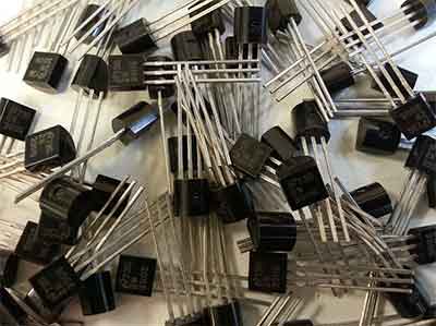
What Types Of Silicon Transistors Are Available?
Silicon Transistor Research
A scientist from an european university asked us to quote the following:
UniversityWafer, Inc. Quoted:
Si Wafer
diameter 150 mm ( 6" )
thickness 525 um
N/As doped
CZ growth
resistivity 0.005 bis 0.01 Ohm/cm
SiO2 layer, high density
dry oxide 300 nm thickness
Single side polished
Quantity: 25 Pieces
Reference #233503
Get Your Quote FAST!
Important Silicon Transistor Terms
- silicon transistors
- transistor technology
- effect transistors
- first transistor
- transistor works
- early transistors
- functional transistor
- silicon chips
- junction transistor
- semiconductor chips
- commercial silicon
- quality silicon
- semiconductor material
- silicon piece
- available silicon
Video: Will Graphene Replace Silicon Transistors?
What Kind of Silicon Transistors Are Available?
If you want to know what kinds of silicon based transistors are available, you've come to the right place. In  this article, you'll learn about NMOS, PMOS, CMOS, and BFET. If you're still confused, here are some general characteristics to help you decide which silicon transistor is right for your needs. Then, you can learn about the benefits and disadvantages of each type and select one that matches your specific needs and preferences.
NMOS Transistors
There are two major types of silicon-based transistors: NMOS and PMOS. NMOS silicon-based transistors have lower on-resistance and higher breakdown strength than PMOS transistors. PMOS transistors are usually used in higher-power amplifiers and power supplies. The difference between NMOS and PMOS transistors can be seen in their collector current value. The NMOS transistors are more efficient in switching current and voltage. They are also less expensive to produce.
NMOS transistors are available in both PMOS and NP-channel configurations. GaN NMOS transistors are a good candidate for power semiconductor applications because they combine low gate leakage with high performance. The GaN NMOS transistor is currently the best choice for high-speed applications, as its low gate leakage makes it a great choice for power-drain switching. Moreover, these transistors are capable of operating at low supply voltages, extending battery life and enabling envelope tracking RF PA.
NMOS silicon based transistors have a wide range of applications. They are primarily used for high-speed switching, and are available in various sizes. Typically, one of the most common NMOS applications involves a semiconductor chip that uses p-channel MOSFETs. They are similar in their construction, but differ greatly in their electrical properties. They are also less expensive and simpler to produce than PMOS transistors.
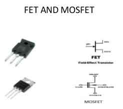
The most common type of transistor is the MOS FET. It is fabricated using controlled oxidation of silicon. The device is then insulated, enabling it to conduct electricity. The change in conductivity with voltage makes it useful for amplifying signals. The MOSFET was invented at Bell Labs by Dawon Kahng in 1959, and it is now the most popular semiconductor device on the market.
Unlike MOSFETs, NMOS transistors have a narrow bandgap, which is a key factor in determining their threshold voltage. The bandgap of the silicon channel and the gate dielectric layers determine their ability to conduct current. The difference in these two materials determines the threshold voltage. In a MOSFET, the dielectric thickness is approximately the same as the silicon channel.
PMOS Transistors
There are several disadvantages to PMOS silicon based transistors. They require several supply voltages, have a relatively large feature size, and are slower to switch than NMOS transistors. These transistors are also known as p-channel MOSFETs. They operate by creating an inversion layer in the n-type transistor body and conducting holes between the p-type terminals. The disadvantages of PMOS are discussed below.
The biggest disadvantage of PMOS transistors is their slow transition from high to low. This is because the transistor's gate provides a low resistance during the transition. As a result, the capacitive charge accumulates at the output very quickly. Additionally, the resistance at the output is greater than the resistance on the negative supply rail, which increases the overall power consumption in the circuit. Another disadvantage of this transistor is its high static power dissipation.
Another drawback of PMOS transistors is their high cost. These devices are primarily used in computer chips. Fortunately, there are cheaper alternatives available. These devices can be found online at electronic stores. And they're widely available. Silicon is a versatile material, with applications in all kinds of fields. The material is abundant and easy to process. It also has good physical properties, including a stable native oxide.
Unlike NMOS transistors, the charge carrier mobility of PMOS transistors is significantly higher. They are more likely to be able to withstand temperature rises of up to 100 degrees. However, their process temperature is low and they don't require any liquid chemicals. Nevertheless, they're still a major challenge to the semiconductor industry. Ultimately, however, the advantages of PMOS over NMOS transistors are worth it.
Power MOSFETs, super-junction power MOSFETs, and IGBTs are all popular options for switching electric power. Power MOSFETs are the least expensive and most common type of semiconductor and are often used in 25-volt to 500-volt applications. Super-junction power MOSFETs are more advanced and have a higher current carrying capacity. IGBTs are the leading midrange power semiconductor.
CMOS Transistors
CMOS silicon based transistors are very common in electronics, but they are not as widespread as bipolar transistors. This is largely due to the difference in their operating voltages. MOS transistors operate from voltages ranging from three to eighteen volts DC, while the more common 5 V TTL is used for digital circuits. But, as transistor sizes and geometric dimensions decreased, CMOS transistors began to operate from voltages as low as one volt.
The main advantage of CMOS on silicon is the ability to shrink the transistor design geometries. The ability to shrink the size of the transistors allows system-level designers to achieve higher performance and reduced power consumption in a small area. The disadvantage of this is that the transistors can no longer scale. This issue has sparked a flurry of activity to find an answer to the scaling challenge. There are now strained Silicon-on-Insulator (SOI) transistors and other new materials.
The CMOS transistor uses silicon oxide as its gate dielectric, but the industry is now exploring other materials with higher dielectric constants. These materials are referred to as High-k dielectrics. These compounds are a great alternative to silicon-based transistors, as they have higher electron mobility and can reduce leakage. Despite the benefits of CMOS transistors, however, CMOS technology has limits and scientists are seeking alternatives.
Carbon nanotubes are also being used for semiconductor devices. The carbon nanotubes have much lower gate capacitance than silicon-based transistors. They have an average gate capacitance of about 70 femtoseconds, which is significantly smaller than the silicon-based transistors. But unlike silicon, carbon nanotubes are not suitable for large-scale integrated circuits. Despite these limitations, researchers are confident enough that they can overcome the challenges presented by silicon.
The CMOS transistors are formed by the intersection of two layers of polysilicon, one on top of the other. Their output (or "out") is connected to a metal layer, which is the other side of the NAND device. Both layers have different resistive properties. The NMOS transistor is typically more expensive, but it is more durable and has a higher switching frequency. In addition, CMOS transistors are more reliable and energy-efficient than their NAND counterparts.
BFET Transistors
Various biomolecules can be detected by SiNW and CNT-based BioFETs. These devices are capable of detecting proteins, enzymes, and hormones without labeling. These devices were initially developed by the Bergveld group, but since then, countless research groups have picked up on the idea and used it to develop new devices. Here are some of the main applications of these transistors.
In this technology, a poly resistance is deposited on the silicon substrate, separated from the top layer. The poly resistance does not cause a voltage drop across the top layer 15 and is protected by the oxide layer 31. Then, all the processing steps are performed with plasma, ensuring minimum damage to the silicon substrate. Moreover, the ion implantation of Be/F and Si allows the realization of self-aligned source and drain regions. In this process, p-channel devices can be achieved. Moreover, a poly resistance can be inserted in place of the n-well resistance.
After a decade of development, a silicon transistor is widely used in computers. Its price is cheaper than its germanium counterpart, and its reliability is superior. However, it has poorer operating characteristics, with higher leakage currents in the "off" state. Moreover, its operating temperature range is limited to 0 to 70 degC, which makes it largely unsuitable for rugged applications.
BFET is a compound semiconductor that can be used to design microwave integrated circuits. These transistors can be used in wireless communication devices. These devices can be used in mobile phones, digital devices, and other RF applications. They also have lower gate leakage than nitride semiconductors. In this way, the transistor can be used in ultra large-scale integrated circuits without having to be separated into two components.
The main differences between graphene transistors and silicon-based transistors lie in their fabrication processes. Graphene is very thin and absorbs 2.3% of white light. Its low-density properties also make it a promising material for solar cells. Additionally, graphene has excellent chemical properties and does not react with other materials, making it a good candidate for chemical sensors and biosensors.
The Field Effect Transistor and Its Benefits
The field effect transistor (FET) is an electronic device that controls the flow of electrons and holes  through a semiconductor path. It has a conductive channel whose size and shape are controlled by the voltage applied across its gate and source terminals. Despite its low energy level, the FET has high conductivity, making it an excellent choice for a variety of applications. However, FETs are not as efficient as semiconductors, making them less practical for high-volume applications.
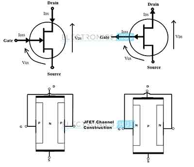
A typical FET functions like a voltage-controlled resistor, with zero resistance at its drain and maximum resistance at its source. In addition, a JFET's gate is always negatively biased relative to its source. The voltage gradient caused by the resistive channel forms a voltage gradient, as it moves from the Drain terminal to the Source terminal. A PN-junction (PN) transistor has a high reverse bias at the Drain terminal and a low reverse bias at the source terminal, resulting in a depletion layer that gradually increases in width as the transistor is biased.
A negative gate-to-source voltage causes the depletion region to expand and close the channel. This results in a large resistance. This condition is referred to as pinch-off. The opposite, positive gate-to-source voltage causes the channel to widen and electrons to flow freely. In the saturation mode, the FET behaves like a constant-current source. This characteristic is useful for amplification. Alternatively, it can act as a voltage amplifier by using its gate-to-source voltage.
Video: FET Transistor Explained
What are The Benefits of a Graphene Transistor?
The graphene transistor is a semiconductor that has recently gained significant attention due to its high  sensitivity and thin channel thickness. It is also being used in biosensors, solar cells, and magnetic sensors. Researchers are pursuing various aspects of graphene transistors to improve their performance. Let's take a closer look at the benefits of this new material. There are many benefits that graphene offers compared to conventional semiconductors.
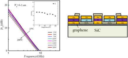
For example, its ability to lower power consumption makes it a viable alternative to conventional semiconductors. In addition, the graphene transistor has a very low oscillation frequency of 29 GHz, making it an excellent candidate for electronic applications. This is because graphene behaves more like a metal than a semiconductor, which increases its usefulness. It is hoped that graphene will become the next generation of semiconductors.
Researchers have developed a technique to fabricate transistors from graphene. Instead of using metals, they used alumina-coated nanowires to serve as gate electrodes. This self-aligning technique makes it possible to produce a graphene transistor with minimum resistivity. Graphene transistors are also capable of controlling the flow of current and preventing the flow of energy. It is a promising step forward in the development of electronics.
Graphene is a sheet of carbon one atom thick. Researchers are currently investigating how to use graphene in solid-state devices. The flakes of graphene are being used to create proof-of-concept devices. The incorporation of graphene is possible if existing fabrication processes are used. If this new material is fully implemented into semiconductors, it can achieve high performance without the problems of conventional silicon-based devices.
Video: Graphene Field Effect Transistor (GFET)
What Is a JFET Transistor?
What is JFET transistors? They are the most common types of transistors, and their functions can be found in a variety of electronic applications. Their primary difference from conventional transistors is the use of two different types of semiconductors - silicon and gallium arsenide. They can also be made with different materials, depending on their applications. Here, we'll discuss the basic characteristics of JFET transistors.

The most fundamental property of JFETs is that their channel resistance is controlled by their drain-source voltage VGS. The greater the reverse voltage VGS, the wider the depletion layer will be. In other words, the drain-source voltage is less important than the gate-source voltage. The voltage between the Source and Drain controls the channel resistance during the saturation and breakdown regions. A higher voltage between the Drain and the Source causes the resistive channel of a JFET to breakdown.
To operate a JFET transistor, the voltage between the source and gate terminals must be less than the current flowing through the circuit. This voltage can be zero if the device is in a conducting state, but a higher voltage may increase the resistance to current flow. In addition, a high voltage can damage the transistor, so it is necessary to know how to use JFET transistors safely. However, they have numerous benefits and applications.
The main body of a JFET is a solid bar made from either P or N-type materials. The channel is connected to the drain by two deposits of material called the gate. When the gate voltage is higher than the source voltage, the channel is narrower and no current can flow. As a result, JFETs are very useful electronic components. Many electronic circuits utilize JFET transistors, including logic switches, oscillators, and amplifiers.
