We are interested in acquiring vicinal Si (100) wafers with a six-degree miscut angle. We would prefer 2" wafers but any larger size is acceptable. We do not have any other doping/thickness requirements. How quickly would we be able to get them if we were to order and what is your pricing for these?
Vicinal Surface and Other Substrates
Vicinal Silicon in Semiconductors
A postdoc requested the following quote:
Please reference #253653 for specs/pricing.
Get Your Quote FAST! Or, buy online and start researching today!
What is Vicinal Silicon Applications?
Vicinal silicon crystallography is the plane the position of which varies very little from that of a fundamental plane of the form.
Researcher requested a the following quote:
We are interested in acquiring vicinal Si (100) wafers with a six-degree miscut angle. We would prefer 2" wafers but any larger size is acceptable. We do not have any other doping/thickness requirements. How quickly would we be able to get them if we were to order and what is your pricing for these?
Our Quote:
Si Wafer
2", 500um, P type, <100> off to <110> 6 degree SSP
Pricing depends on quantity.
Vicinal silicon It is a relatively new material, first identified in 1824 by Swedish chemist Jons Jacob Berzelius. Since then, scientists have worshiped it as a powerful substance with many uses. In the late 1970s and early 1980s, silicon transistors replaced vacuum tubes in electronic devices. Today, it remains a key material in semiconductors. Listed below are some interesting facts about the material.
It's a material that is incredibly useful in electronics. Its atomic structure allows it to be used as a template for controlled structures. It is created by cutting a silicon crystal at a small angle from its crystal plane. The surface is trying to maintain its preferred orientation, but it can't. When the miscut angle causes the silicon crystal to sag, it is forced to form atomic steps. The resulting surfaces are low-dimensional and have a very large surface area.
The structure of Vicinal Silicon is a 7x7 reconstruction of the surface. The seven atomic layers are bonded in a layered structure, and the atomic chains are formed through the alignment of electrons. This means that a single crystalline silicon rod is a single atom. These atomic layers are formed by arranging the atoms in the 111 directions. The material's high-temperature dependence allows it to be used in electronics.
It has a stepped surface that is used in high-temperature environments. Stepped surfaces are formed by cutting a silicon crystal at a small angle from a stable crystal plane. The miscut forces the silicon to retain its preferred orientation. When this happens, it is forced to form atomic steps. These terraces are separated by atomically flat stretches. The width of these terraces is determined by the angle at which the surface was cut.
Its atomic steps are formed by a 7x7 reconstruction of the surface of the silicon atoms. It is a high-dimensional material and is a good example of a semiconductor. It is highly conductive, with an extremely low melting point. This property makes it a very good material for electronics. This material has several advantages. If a transistor has a high-speed processor, it will be much faster and more reliable.
Stepped surfaces are very useful as templates for controlled structures. They are formed by cutting silicon crystals at an angle to their highly stable crystal plane. The silicon surface will try to maintain its preferred orientation even if it is cut at a small angle. When this happens, the atoms are forced to form atomic steps. These atomic steps are separated by atomically flat terraces. The angle of the miscut is the determining factor for the width of these terraces.
Steps are a useful material in electronics. These structures are made by slicing the crystalline silicon at an angle. The resulting structure is a highly stable monolayer. It is also a good material for electronic components and devices. Its atomic steps are the best material for electronic products. They are very important for electronic devices and components. But how is it created? What is Vicinal Silicon? Amorphous silicon is a very useful material that has several properties.
When the silicon crystals are stepped, they act as templates for controlled structures. The process of making a stepped silicon surface requires cutting the silicon crystal at an angle similar to that of a graphene surface. This angle forces the silicon to form atomic steps. The atomic steps are separated by atomically flat terraces. The angle of the miscut is the size of the terraces. Once formed, the crystalline silicon surface is used to make electronic devices and components.
The crystalline silicon structure is a stepped surface. It has a high surface area and is perfect for electronic components. Its atomic steps can also be used as templates for controlled structures. When a stepped silicon surface is heated, it forms a 7Z7 pattern. The 7x7 surface is a semiconducting material, while a 7x7 is a metallic material. This material is used for semiconductors and other electronic devices.
Video: Vicinal Surfaces Explained
Vicinal Silicon Carbide Substrates
A corporate researcher requested the following quote:
Would you kindly send me a details spec. on vicinal 6H-SiC substrates (Si-face, 4-6 degree off toward [112n]? Our research interest require the atomically defined step-terrace structure on Si-face SiC.
Reference #96059for specs and pricing.
Vicinal Germanium Substrates
Do you have or can you source vicinal germanium (100) 1deg offcut. This is quiet specialised I know but thought.
Reference #128328 for specs and pricing.
What is Vicinal Silicon Wafers?
Vicinal silicon wafers typically have 2-3 degrees relative to the substrate;s crystal planes. This allows for a better surface finish and improved crystal quality. These wafers are commonly used in semiconductor manufacturing, as they can be processed more efficiently than wafers cut perpendicular to the crystal planes.
The Vicinal Silicon interface is a key component of a semiconductor device. Moreover, 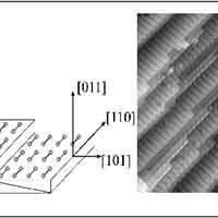 the material has several useful properties, such as high temperature resistance and electrical conductivity. In this study, the vicinal interface was studied using the same technique. The results showed that the surface of the interface is rough and contains a small amount of defects. These features have important implications for the manufacturing process of semiconductors. In addition, these findings provide insight into the origin of the material's chemical composition.
The atomic scale roughness in silicon crystals limits the electron mobility and reliability of the device. The area depicted in the image is about 400x400 nm. The atomic staircase steps are 0.3 nm high and are 15-17 nm wide. To illustrate the effect of the surface roughness, the vertical axis is stretched by a factor of 15 to show the staircase. The X-ray images of the vicinal silicon spectroscopy are displayed on the right.
The area shown in the image is 400x400 nm. The atomic staircase steps are 0.3 nm tall. The steps are 15-17 nm wide. The image is a derivative of a STM and shows the illumination from the left. The downhill is to the right and the steps are black lines. There are several ways to examine the vicinal silicon spectroscopy. For the most detailed analysis, the STM data must be analyzed under these conditions.
The vicinal silicon spectroscopy image is a representation of the atomic structure of the surface. The atomic surface is made of seven-layer silicon crystals. The silicon atoms have a uniform structure. The atomic layer is smooth, but it is rough at the atomic scale. This roughness constrains the electron mobility and reliability of SiC based devices. This is an important factor for the design of ICs and nanoscale vicinal Silicon
The vicinal silicon spectroscopy images are not necessarily representative of the actual vicinal silicon. However, the atomic steps on the surface are the result of a miscut of a single silicon crystal. The angle of the miscut causes asymmetry in the atomic structure and forces the surface to adopt a preferred orientation. The atomic step spectroscopy image is an accurate representation of the atomic structure of the vicinal silicon.
Stepped silicon surfaces are useful as templates for controlled structures. These atomic-scale surfaces are formed by cutting a silicon crystal at an angle to its highly stable crystal plane. In the process, the surface is forced to form atomic steps because of the miscut angle. These terraces are separated by atomically flat terraces. The miscut angle also determines the height and width of the atomic steps. The stepped silicon image has a high degree of angular stability.
In addition to atomic-scale features, vicinal Silicon features a high degree of roughness, which limits electron mobility. The structure is a stepped silicon image in which atomic steps are separated by atomically flat terraces. The size of a vicinal silicon sample depends on the miscut angle. The vicinal silicon is a low-dimensional material that is relatively rigid and has an inherent flexibility.
The surface is made up of seven atomic-scale steps. The stepped silicon surface is made by cutting a silicon crystal at a small angle to its highly stable crystal plane. As a result, the silicon surface attempts to maintain its preferred orientation. The miscut causes the surface to form atomic-scale steps. The terraces are separated by atomically flat terraces. The miscut angle also determines the width of the stepping silicon structures.
The atomic-scale steps are created by dividing the surface into terraces. The vicinal Silicon is also called stepped silicon. The atomic-scale stepped surface has been discovered using the spectroscopy of the vicinal Silicon. Its height and width is measured in nm. The stepped silicon image is a sample of the vicinal Silicon. If you want to study the vicinal side of a vicinal Silicon, the image on the right shows the illumination from the left.
What is Stepped Silicon Surface?
A stepped silicon surface is a template for controlled structures. It is formed by cutting 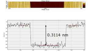 single crystal silicon at a small angle to the highly stable crystal plane. This miscutting causes the surface to attempt to maintain its preferred orientation. The result is a stepped structure. The atomic steps are separated by terraces that are atomically flat. The width of the terraces depends on the angle at which the surface is cut.
This paper studied the morphology of a textured silicon substrate by anisotropic texturing with KOH. The process parameters determined the degree of texturing and the final surface morphology. AFM images were analyzed with Nanoscope and Gwyddion software to reveal the depth, section, and step height. In contrast, the morphology of a single point defect is difficult to visualize. In this paper, we simulated the effects of these processes on the atomic-scale structure of a stepped silicon surface.
A simulation of a low-energy implant on a silicon stepped surface reveals that atoms are trapped by vacancies in the surface. In this scenario, the bombarded atom has a realistic vicinal structure with one step edge. The implanted Ar or Si produces a low-kinetic energy atom that produces a damaging event. A detailed simulation indicates the total etching of the first two layers of silicon, as well as the ejection of the implanted Ar. Moreover, these features hold even when the atom moves in opposite directions.
The structure of the silicon stepped surface was investigated through the use of atomic force microscopy. The researchers found that the atomic force microscopy imaging showed that the stepped surface has two dimensional (D-spacing) features. These structures are highly complex and require the use of a high-precision microscope. To observe their morphology, the simulations were carried out at different temperatures. There are several types of these stepping surfaces.
These structures were created by bombarding a silicon stepped surface with a low-energy atom. The simulations were performed under ambient conditions and under various conditions. The atomic force microscopy images revealed the formation of the stepping surfaces. The authors also found that the stepped surfaces are more prone to abrasion than non-stepped surfaces. In addition, the experiment showed that the atoms in the stepping surface have an energy barrier of at least 0.3 MeV.
The area in the image shown on the right is 400x400 nm, while the terraces are 15-17 nm in width. The steps in the silicon stepped surface are 0.3 nm high and are located on the surface. The simulations show that the atoms in the atomic staircases are emitted from the surfaces by means of a spherical molecule. The structure of the stepped silicon stairway is asymmetrical.
These experiments demonstrate how the atomic steps are formed in a stepped silicon surface. The steps are located near the atomic steps and are characterized by a vicinal structure of two steps. The asymmetric structure of the stepping surface allows the atoms to interact with each other at a low temperature. Aside from these features, the STM images were produced under ambient conditions. The atomic stepping process can also be carried out in vacuum.
Aside from this, the surface morphology of a stepped silicon surface is also a key to understanding the structural properties of nanostructures. In addition to atomic steps, a stepped surface is a textured surface that is produced by a high-energy process. A stepping process will result in a textured surface whose atomic step height is a function of the atomic step length.
Despite these limitations, atomic stepping is an effective method to produce a stepped surface. Using this technique, the atomic steps are shaped with one step edge per atom. The results of the simulations show that the atomic steps are shaped like a staircase and have a vicinal structure that is consistent with the structure of the stepping surfaces. The metric of the stepping is based on the area of the stepped surface.
The chemistry behind this stepping is a fascinating way to study the structure of silicon. Its growth rate is proportional to the size of the step. The measured atomic steps are circular, but they are not stationary. A stepped surface in silicon is called a stepped surface. However, a stepped-surface is a layered surface with multiple layers. This surface is a layered structure, with a slit in the middle.
What is a Vicinal Surface?
One area of research is the characterization of vicinal surfaces. These are low-dimensional materials that have regular arrangements of atomic steps and can be functionalized for technical purposes. In addition, vicinal surfaces contain well-defined defects structures and are excellent nuclei for low-dimensional nanostructures. Furthermore, the concentration of vicinal surfaces can be controlled by adjusting the inclination angle of the substrate. These properties are crucial for controlling the electronic and chemical properties of nano-objects and making them usable.
- Regularly speaced low Miller index terraces separated by monoatomic steps
- Obtained by cutting the crystal at an angle "slightly" off the low Miller inded
A vicinal surface is a thin film with a normal deviating from the main crystallographic  axis. A vicinal surface is a material with a terrace-like morphology. It also has special adsorption sites adjacent to steps or terraces. These special adsorption sites are important for catalytic reactions. The morphology of a compound surface can also change its stoichiometry, showing deviations from bulk stoichiometry.
A vicinal surface does not have a regular staircase-like morphology; instead, it has a terrace-like morphology. The morphology of the vicinal surface is shaped by the occurrence of special adsorption sites adjacent to steps. The presence of these sites may be important for catalytic reactions. In some cases, a vitiated surface will have a pronounced deviation from its bulk stoichiometry, resulting in localised reactions and segregation of the adsorption site.