What Silicon Wafer Should I Use for My Research?
What Silicon Wafer Spec Should I use?
We help scientists find the best silicon wafer for their research. Our engineers have decades of experience helping PHD in academia and scientists through the world's industries from start up to fortune 500 companies and government labs as well.
Send us your question. We'll provide the quote!
Get Your Quote FAST! Or, Buy Online and Start Researching Today!
What is a Silicon Wafer?
Silicon is the material used in the manufacture of semiconductors and is contained in electronic devices that improve people's lives. Silicon is mainly used as a semiconductor in technology and electronics. It is one of the most widely used elements in our universe, whether in electronics or in materials such as ceramics, glass, metals, plastics or even plastics.

Silicon Wafer With Thermal Oxide on The Surface
Most people would probably never have seen a real silicon wafer in their lives if it were not the most common form of silicon.It also consists of subtle surface irregularities, making it the flattest object in the world, but it is also the perfect substrate material for modern semiconductors. This super flat disc is refined to a mirror-like surface and is also the most common form of silicon wafers.
During the entire growth process, doping agents can be used to alter the purity of the silicon wafer depending on its manufacturing purpose. These impurities can alter the electronic properties of silicon, which are indispensable depending on the production purpose. Different methods are used in silicon production, including the use of different materials such as silicon dioxide, silicon nitride and silicon oxide.
Silicon doping agents that can be added during the growth process are aluminum, boron, nitrogen, indium and gallium. Silicon wafers can also be considered degenerated or extrinsic, depending on whether or not the silicon wafer was added during doping. Degenerated semiconductors are used as conductors, while lightly or relatively doped semiconductors are called "extrinsic" semiconductors.
What are Silicon Wafers Used for?
Silicon is the best and most widely used substrate to fabricate semiconductor, although other conductors are used for more specific applications. Silicon is an excellent option because its electric current can flow through silicon much faster than any other conductor.
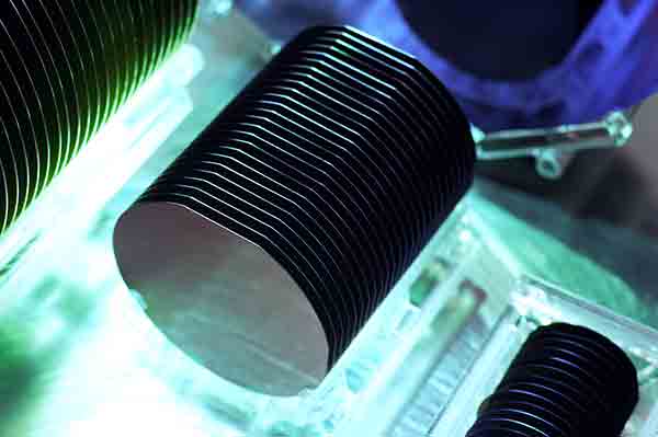
Stack of Silicon Wafers
Semiconductors such as silicon wafers can be used to produce chips (microchips) and electronic devices.Due to the uniqueness of the electric current on silicon wafers, semiconductors are used to produce ICs (integrated circuits). Ics are the basis for a wide range of electronic devices such as computers, televisions, cameras and other electronics.
Simply put, an integrated circuit is a network of a variety of electronic elements that are brought together to perform a specific function. The silicon wafer is the main element in integrated circuits, but it is not the only part of the circuit.
The wafer is a thin disk made of semiconductor material that serves as a substrate for microelectronic devices mounted on it. Silicon is the key platform for semiconductors and devices, but it is used in a variety of applications that people can only dream of. Although it can be easy to be associated with silicon wafers, they are actually much closer than you might think.
Silicon wafer production is operated by a number of different companies including Intel, Samsung, Intel Corporation and Samsung Electronics Company.