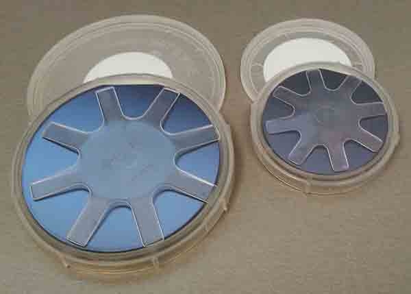
Gallium Arsenide (GaAs) Wafers
Gallium Arsenide (GaAs) Substrates (Buy Online and Save!)
Gallium Arsenide competes with Silicon for many commericial grade electronics and solar applications. But at nearly 1,000 times greater expensive than silicon (comparing 200mm diameters). GaAs wafers have taken a back seat to Silicon. But researchers are devising new methods to bring the costs down.
Get Your Quote FAST!
Gallium Arsenide Applications Include:
Microwave frequency integrated circuits
- Monolithic microwave integrated circuits
- Infrared light-emitting diodes
- Laser Diodes
- Solar Cells
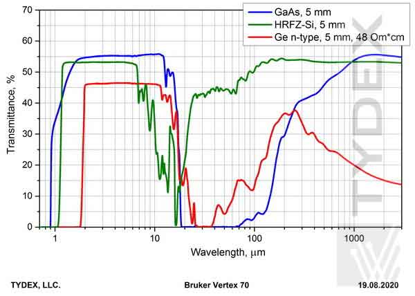
- Optical Windows
Our GaAs are Vertical Gradient Freeze (VGF) Grown and Liquid Encapsulated Czochralsky (LED) Grown GaAs.
What is VGF Gallium Arsenide?
What is VGF Gallium Arsenide? It is a semiconductor material that is grown using the Vertical Gradient Freeze method. It is an ideal semiconductor material for use in semiconductor devices and other electronic applications. It is used for the production of light-emitting diodes, which are used in optical communications, control systems, and computer systems. The growth of VGF Gallium Arsenide involves the use of high-purity 6N input material. The process also involves the addition of high-concentration dopants to achieve the desired concentration level.
Compared to the conventional VB process, the VGF method provides a higher electron velocity and mobility. Its high band gap and high radial uniformity make it suitable for a wide range of applications, including RF, optical, and hybrid devices. Unlike silicon, however, it is less sensitive to overheating and has lower parasitics than silicon. It can be fabricated into thin-film transistors, which is used in wireless systems, solar panels, and high-voltage electronics.
The VGF method is also known as the VB method. This method is widely used in semiconductor applications. It grows single crystals with very low dislocation densities and high electrical resistivity. The GaAs crystals fabricated by this method have an EPD of below five thousand/cm-2. What is VGF Gallium Arsenide? Here is an overview. This article will provide answers to frequently asked questions and provide a more complete understanding of this complex semiconductor material.
VGF Grown GaAs advantages include:
- Scalability
- Low stress
- High mechanical strength
- Defect rate that is orders of magnitude lower than conventional compound semiconductor crystal growth processes.
Compared to less expensive Silicon, Gallium Arsenide superior properties include its higher saturated electron velocity and higher electron mobility.
GaAs's higher electron mobility allows GaAs transistors to function at frequencies in excess of 250 GHz. GaAs devices rarely overheat due to its wider energy bandgap. GaAs also tends to create less noise in electronic circuits than silicon devices, especially at high frequencies. This is a result of higher carrier mobilities and lower resistive device parasitics.
These superior properties are compelling reasons to use GaAs circuitry in mobile phones, satellite communications, microwave point-to-point links and higher frequency radar systems. It is also used in the manufacture of Gunn diodes for the generation of microwaves.
Liquid Encapsulated Czochralsky (LEC) Gallium Arsenide
The term "liquid-encapsulated" has been associated with gallium arsenide, a compound with a high melting point. As a result, it can be used for a variety of applications, including solar cells and batteries. The term also applies to a variety of other metal compounds, such as aluminum and antimony. In addition to gallium arsenide, Liquid Encapsulated Czochalsky is also known as LICzAGAS.
Liquid Encapsulated Czochrally-encapsulated Czochralsky technology is a type of process used for the  growth of single crystals of gallium arsenide. It has many advantages over previous techniques, including simplicity and ease of operation. It can be applied for a wide range of applications, including medical devices. Here's a look at how it works.
A single crystal of GaAs can be grown using the LEC technique. This process produces a small number of dislocations in a single crystal. This process is used for the production of tiny-diameter GaAs devices. The disadvantage of the process is that it is labor-intensive and expensive. However, this method provides several benefits over the previous methods.
A typical Liquid Encapsulated Czochrialsky GaAs device is a thin, glass-like material. Its crystalline structure allows for a high-temperature liquid seal, ensuring a strong seal. Moreover, Liquid Encapsulated Czochraly GaAs can be used for various purposes, including high-voltage applications.
Liquid Encapsulated Czochralsky (LED) Grown GaAs
We have a large selection of LEC grown Gallium Arsenide Wafers. Please send us your specs.


