
Request Wafers to Your Required Specification
UniversityWafer supplies silicon wafers and other research substrates with application-specific dimensions, electrical properties and surface finishes. Include the standard designation and revision, applicable wafer category, numerical tolerances and documentation requirements with your request. Confirm the agreed requirements for the selected material before ordering.
Let us know what you need for an immediate quote!
Get Your Quote Fast! Or Buy Semiconductor Wafers Online and start researching today!
What Are SEMI Standards?
SEMI publishes industry specifications, test methods, guides and practices for semiconductor materials, equipment and manufacturing. A specification describes requirements, while a test method describes how a property is measured. Identify both when they are needed to compare supplier results.
SEMI M1 addresses polished single-crystal silicon wafers, including ordering information, dimensions and certain other properties. Its scope is specific: related wafer types can require separate standards. Refer to the official SEMI M1 catalog entry for the document scope and available revisions.
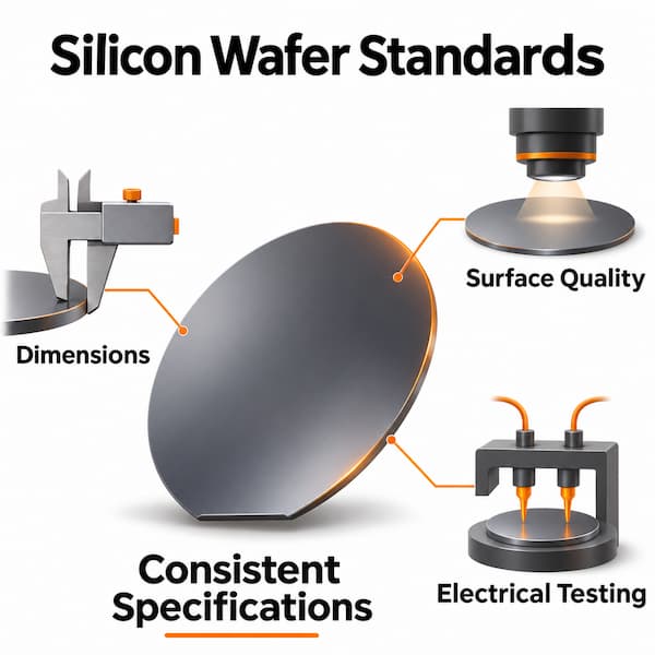
Silicon Wafer Specifications to Include in an Order
| Parameter | What to specify |
|---|---|
| Diameter and thickness | Nominal dimensions, units and tolerances; identify the wafer category. |
| Orientation and edge features | Crystal orientation, flat or notch requirements, and any orientation tolerance. |
| Electrical properties | N-type or p-type, dopant and resistivity range in Ω·cm. |
| Geometry | Limits and measurement conditions for total thickness variation (TTV), bow and warp. |
| Surface finish | Single-side or double-side polish, roughness, surface inspection and defect criteria. |
| Coatings and layers | Thermal oxide, nitride or other film thicknesses, coated sides and tolerances; specify SOI layers separately. |
| Verification | Test method, sampling, acceptance criteria, lot identification and requested documentation. |
A numerical limit and a measurement method serve different purposes. Agree on both where the result determines acceptance. Coatings and thermal processing can also change wafer geometry, so specify whether limits apply before or after processing.
Examples of Wafer and Equipment Standards
The following examples summarize subject areas, not the full requirements of the standards. Verify scope, revision and applicability in the publisher’s catalog.
- SEMI M1: Polished single-crystal silicon wafer specifications.
- SEMI M8: Polished monocrystalline silicon test wafers.
- SEMI M24: Polished monocrystalline silicon premium wafers; this is not a general orientation-flat standard.
- SEMI MF84: Silicon wafer resistivity measured with an in-line four-point probe.
- SEMI MF1390: Bow and warp measured by automated noncontact scanning.
- SEMI E10: Equipment reliability, availability, maintainability and utilization; this is an equipment standard rather than a wafer dimensional specification.
The SEMI standards FAQ explains document access and the transfer of certain former ASTM semiconductor methods into the SEMI MF series. Check the current designation and status when a legacy drawing cites an ASTM method.
SEMI vs. JEDEC, ASTM and ISO
- SEMI: Materials, wafer requirements, manufacturing equipment and associated measurement practices.
- JEDEC: Microelectronics standards, including device, memory, packaging and reliability topics.
- ASTM International: Materials and test-method standards. Some historical semiconductor methods moved to SEMI; confirm which publisher maintains the method you need.
- ISO 9001: Requirements for an organization’s quality management system. Quality-system certification does not replace a wafer’s agreed dimensional, electrical or surface requirements.
These organizations publish standards with different scopes. Identify the document that applies to your material or process instead of treating the organizations’ names as interchangeable wafer grades.
How to Request Wafers with Defined Acceptance Criteria
- Define the substrate: Provide material, diameter, thickness, orientation, conductivity type, dopant, polish and quantity.
- Identify the reference: Include the standard designation, revision and relevant category, plus your drawing when applicable.
- State the required limits: List numerical tolerances and any exceptions or custom dimensions.
- Agree on verification: Specify test methods, sampling and required certificates or measurement reports.
- Confirm processing and handling: Include coatings, cleaning, packaging, labeling and any requirements that apply after processing.
Get Your Quote Fast! Request wafers to your specifications or browse semiconductor wafer inventory.
SEMI Wafer Standards Questions
Does “SEMI standard” describe one wafer specification?
No. Ask for the specific standard, revision, wafer category and agreed limits. The phrase alone does not identify every electrical, dimensional and surface requirement.
Are test wafers covered by the same requirements as prime wafers?
Do not assume they are. SEMI lists separate standards for polished test wafers and other wafer categories. Match the document scope and agreed requirements to the material being purchased.
Can a custom wafer use standard test methods?
A custom drawing can specify nonstandard dimensions alongside agreed measurement methods. Document each requirement and exception in the purchase specification.
Where can I obtain the full standards?
Use the publisher’s official catalog or an authorized subscription. This page provides an educational overview; the referenced documents contain the complete requirements.