
Find the Right Semiconductor Wafer
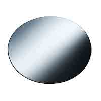 UniversityWafer supplies a wide selection of
semiconductor wafers and substrates
for research, prototyping, process development, and device fabrication.
UniversityWafer supplies a wide selection of
semiconductor wafers and substrates
for research, prototyping, process development, and device fabrication.
Available materials include silicon wafers, SOI wafers, silicon carbide wafers, sapphire wafers, gallium arsenide wafers, and other advanced substrates.
To receive an accurate quote, include as many specifications as possible, such as:
- Wafer material and diameter
- Thickness and crystal orientation
- Conductivity type, dopant, and resistivity
- Single-side or double-side polish
- Oxide, nitride, metal, or epitaxial layers
- Quantity and delivery requirements
Our team can help identify a suitable wafer when your final specifications are still being developed.
Get Your Semiconductor Wafer Quote FAST! Complete the form below with your specifications and quantity. You can also buy wafers online and start your research today.
What Is a Wafer?
A wafer is a thin, flat disc made from a semiconductor material or another engineered substrate. Wafers provide the smooth, uniform surface needed to fabricate microchips, sensors, electronic components, optical devices, and other advanced technologies.
The most widely used semiconductor substrate is the silicon wafer. However, researchers also use silicon-on-insulator (SOI) wafers, silicon carbide wafers, sapphire wafers, gallium arsenide wafers, germanium wafers, and other specialized materials.
Wafer diameter, thickness, crystal orientation, resistivity, dopant, surface finish, and deposited films can all be customized for a particular experiment or fabrication process. Common wafer diameters include 2 inch, 3 inch, 4 inch, 100 mm, 150 mm, 200 mm, and 300 mm.
How Are Semiconductor Wafers Made?
Semiconductor wafer manufacturing commonly begins by growing a high-purity single-crystal ingot. The silicon crystal ingot or other crystal is sliced into thin discs, edge-ground, lapped, polished, and thoroughly cleaned. These steps produce a wafer with the flatness, surface quality, and cleanliness required for semiconductor processing.
Depending on the application, the wafer may then receive additional processing such as thermal oxidation, thin-film deposition, epitaxial growth, photolithography, etching, ion implantation, metallization, or wafer bonding.
What Are Wafers Used For?
Wafers serve as the starting substrate for microelectronics and many other research and manufacturing applications. Their flat, controlled surfaces allow engineers to build microscopic device structures one layer at a time.
Common wafer applications include:
- Integrated circuits, microprocessors, and memory devices
- MEMS sensors, actuators, microphones, and accelerometers
- Power semiconductor devices and high-temperature electronics
- Photonics, lasers, LEDs, and optical detectors
- Solar cells and energy research
- Quantum devices and nanotechnology
- Thin-film deposition and materials characterization
- University laboratory training and semiconductor process development
Popular Types of Wafers
The best wafer material depends on the electrical, mechanical, thermal, and optical requirements of the device.
- Silicon wafers — used for integrated circuits, MEMS, sensors, thin films, and general semiconductor research.
- SOI wafers — used for MEMS, RF electronics, photonics, and advanced transistor fabrication.
- Silicon carbide wafers — selected for power devices, high-temperature electronics, and wide-bandgap semiconductor research.
- Sapphire wafers — used for LEDs, RF devices, optical research, and gallium nitride epitaxy.
- Gallium arsenide wafers — used for high-frequency electronics, lasers, photodetectors, and solar cells.
- Germanium wafers — used for infrared optics, detectors, epitaxy, and advanced semiconductor devices.
Why Are Silicon Wafers Important?
Silicon is the most commonly used semiconductor wafer material because its electrical properties can be precisely controlled through doping. Silicon can support conductive device regions while its native oxide, silicon dioxide, provides an excellent insulating layer for semiconductor fabrication.
Silicon also offers several important advantages:
- High thermal stability: Silicon has a melting point of approximately 1414 °C and can tolerate many high-temperature fabrication processes.
- Useful thermal properties: Silicon conducts heat effectively enough for many electronic and microsystem applications.
- High-quality native oxide: Silicon dioxide can be grown directly on the wafer to create insulating, masking, and passivation layers.
- Controlled electrical properties: Silicon wafers are available as intrinsic, n-type, or p-type material across a wide range of resistivities.
- Commercial availability: Silicon wafers are produced in many diameters, orientations, thicknesses, surface finishes, and doping specifications.
How Do You Choose the Right Wafer?
When requesting a wafer quote, researchers should specify the material, diameter, thickness, crystal orientation, conductivity type, dopant, resistivity, surface finish, quantity, and any required oxide, nitride, metal, or epitaxial layers.
UniversityWafer supplies research and production quantities of silicon, SOI, sapphire, silicon carbide, gallium arsenide, germanium, glass, quartz, epitaxial, and coated wafers. Visit the UniversityWafer online store or submit your specifications to request a quote.
Explore Semiconductor Wafers & Research Substrates
- Silicon Wafers
- SOI Wafers
- Epitaxial Silicon Wafers
- Thermal Oxide Wafers
- Silicon Nitride Wafers
- Sapphire Wafers
- Silicon Carbide (SiC) Wafers
- Gallium Arsenide (GaAs) Wafers
- GaN on Sapphire
- Germanium Wafers
- Glass Wafers
- Fused Silica Wafers
- Single Crystal Quartz
- ITO Glass Wafers
- Semiconductor Materials
- Research Substrates
- Thin Film Deposition Wafers
- MEMS Wafers
- Photolithography
- Wafer Fabrication Process