
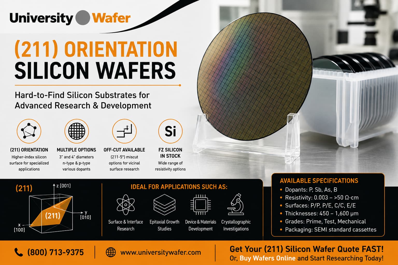
Hard-to-Find (211) Silicon Wafers in Stock
UniversityWafer supplies specialized (211) orientation silicon wafers for research, development, and advanced materials studies. These higher-index silicon substrates are less common than standard (100), (110), and (111) wafers and can be difficult to source in specific diameters, dopant types, resistivity ranges, and surface finishes.
Available specifications may include n-type and p-type silicon, phosphorus (P), antimony (Sb), arsenic (As), and boron (B) doping, as well as Float Zone (FZ) material. Wafers can also be supplied with different thicknesses, polished or etched surfaces, and selected orientation tolerances depending on inventory.
Why Use (211) Silicon?
The (211) crystallographic plane presents a different surface atomic arrangement than commonly used silicon orientations. This makes (211) substrates useful for specialized experiments involving surface structure, epitaxial growth, interface formation, thin-film deposition, and crystallographic studies.
Some available wafers also include intentional off-cut or miscut orientations. These substrates can be useful for research involving vicinal surfaces, step formation, and orientation-sensitive material growth.
Specify the Wafer You Need
For the best match, include your required wafer diameter, thickness, conductivity type, dopant, resistivity, crystal orientation, orientation tolerance, surface finish, and quantity. If your project requires a specific off-cut angle or miscut direction, include that information in your request as well.
Get Your (211) Silicon Wafer Quote FAST!
Or,
Buy Wafers Online
and Start Researching Today!
(211) Orientation Silicon Wafers
Silicon (211) wafers are single-crystal silicon substrates cut so that the wafer surface is nominally parallel to the (211) crystallographic plane. Unlike the more commonly used (100), (110), and (111) orientations, (211) is a higher-index silicon surface and is primarily used for specialized semiconductor, surface-science, epitaxial-growth, and crystallographic research.
UniversityWafer offers hard-to-find (211) silicon substrates in several diameters, dopant types, resistivity ranges, thicknesses, and surface finishes. The inventory below includes phosphorus-, antimony-, arsenic-, and boron-doped silicon, as well as Float Zone (FZ) material for applications where researchers require specific electrical or crystallographic properties.
What Does a (211) Silicon Orientation Mean?
The designation (211) is a Miller-index notation describing the crystallographic plane parallel to the wafer surface. Because silicon has a diamond-cubic crystal structure, changing the wafer orientation changes the atomic arrangement presented at the surface. This can influence surface reconstruction, adsorption, interface formation, epitaxial nucleation, and other surface-dependent phenomena.
For this reason, (211) silicon is particularly useful when a research project requires a surface geometry that differs from standard (100), (110), or (111) silicon. High-index silicon surfaces are frequently investigated in fundamental surface science and materials research where atomic-scale surface structure is important.
(211) Silicon with an Off-Cut
Some wafers listed below are specified as [211-5°]. This indicates that the supplied crystal orientation includes an intentional angular offset, or miscut, of approximately 5 degrees from the nominal (211) orientation according to the inventory specification. Miscut substrates are often selected when researchers want to investigate stepped or vicinal surfaces, epitaxial growth behavior, or other orientation-sensitive processes.
The exact miscut direction and angular tolerance should be confirmed when those parameters are important to an experiment, because the miscut angle alone does not completely define the crystallographic direction of the tilt.
Available (211) Silicon Wafer Specifications
The table below shows examples of UniversityWafer's (211)-orientation silicon inventory. Specifications may include nominal crystal orientation, orientation tolerance, diameter, thickness, dopant, resistivity, surface finish, and wafer grade. Please confirm current availability and required specifications when requesting a quote.
| Item | Type/Dopant | Orientation | Dia. | Thickness (µm) | Surface | Resistivity (Ω·cm) |
|---|---|---|---|---|---|---|
| SEMI Test, 1 Flat, Empak Cassette — Wafers can be polished for an additional fee | ||||||
| 4975 | n-type Si:Sb | [211] ±0.5° | 4" | 1,500 ±15 | P/P | 0.01–0.02 |
| Prime, 1 Flat, Empak Cassette | ||||||
| F975 | n-type Si:Sb | [211] ±0.5° | 4" | 1,600 | C/C | 0.01–0.02 |
| 5753 | n-type Si:P | [211-5°] ±0.5° | 3" | 508 | P/P | FZ >50 |
| 5752 | n-type Si:P | [211-5°] ±0.5° | 3" | 508 | P/P | FZ 25–75 |
| 5750 | n-type Si:P | [211-5°] ±0.5° | 3" | 508 | P/P | FZ 25–75 |
| 5754 | n-type Si:P | [211] ±0.5° | 3" | 1,016 | P/P | FZ 25–75 |
| 5755 | n-type Si:P | [211-5°] ±0.5° | 3" | 508 | P/P | FZ 25–75 |
| 5756 | n-type Si:P | [211-5°] ±0.5° | 3" | 508 | P/P | FZ 25–75 |
| 5757 | n-type Si:P | [211-5°] ±0.5° | 3" | 508 | P/P | FZ 25–75 |
| 5758 | n-type Si:P | [211] ±0.5° | 3" | 508 | P/P | FZ 25–75 |
| SEMI Test, 1 Flat, Empak Cassette | ||||||
| 5759 | n-type Si:P | [211] ±0.5° | 3" | 1,016 | P/P | FZ 25–75 |
| 5760 | n-type Si:P | [211] ±0.5° | 3" | 1,016 | P/P | FZ 25–75 |
| 5331 | p-type Si:B | [211] ±0.5° | 3" | 525 | P/P | >10 |
| SEMI Prime, 1 Flat, Empak Cassettes (7–8 wafers) | ||||||
| D331 | p-type Si:B | [211] ±0.5° | 3" | 525 | P/E | >10 |
| SEMI Prime, 2 Flats, Empak Cassette | ||||||
| 1912 | n-type Si:As | [211] ±0.5° | 3" | 550 | E/E | 0.0030–0.0042 |
| 11P2 | n-type Si:P | [211] | 3" | 450 | P/P | 50–65 |
Choosing a (211) Silicon Wafer
When selecting a wafer, consider more than crystal orientation. Dopant species and resistivity determine the electrical characteristics of the bulk silicon, while thickness and surface preparation can affect handling, processing, interface quality, and experimental design. Float Zone silicon is also available in several of the listed specifications for research requiring FZ-grown material.
If your experiment requires a specific orientation tolerance, miscut direction, resistivity range, surface finish, wafer thickness, or dopant concentration, provide those requirements when requesting a quote so the substrate can be matched to your application.
Related Silicon Wafer Resources
Learn more about silicon crystal orientation, wafer growth methods, grades, and other substrate options for semiconductor and materials research.
- Silicon Wafers & Substrates
- Silicon Wafer Crystal Orientation Guide
- (100) Orientation Silicon Wafers
- (110) Orientation Silicon Wafers
- (111) Orientation Silicon Wafers
- Float Zone (FZ) Silicon Wafers
- Czochralski (CZ) Silicon Wafers
- Prime Grade Silicon Wafers
- Test Grade Silicon Wafers
- Mechanical Grade Silicon Wafers
- Request Custom Silicon Wafer Specifications