Patterned ITO Wafers
UniversityWafer supplies indium tin oxide (ITO) coated glass substrates
for research requiring transparent conductive surfaces, custom patterns,
controlled sheet resistance, and optical-quality substrates.
Patterned ITO can be useful for optical calibration targets, sensors,
transparent electrodes, microfabrication, lithography, displays, and
electro-optical research.
An application scientist requested the following custom configuration:
We are developing a calibration product for optical microscopes and require
a specific ITO pattern on an optically flat glass substrate. The desired
geometry is based on a 1951 USAF resolution target, with ITO thicknesses
ranging from approximately 10 nm to 100 nm.
Optical flatness is also important, with a target specification comparable
to a high-quality parallel optical flat.
Reference #187783 for specifications and pricing.
For custom patterned substrates, please provide the desired pattern,
substrate material, dimensions, ITO thickness, sheet resistance,
flatness requirement, and quantity.
ITO Wafers for Spin-Coating and Spin-Curve Testing
ITO-coated glass can also serve as a conductive test substrate for
spin coating, resist characterization, polymer coating, and
thin-film process development.
A PhD researcher requested:
Basic 6-inch-diameter ITO-coated glass wafers for spin-curve testing.
The researcher did not require a specific substrate thickness and preferred
a standard, economical configuration suitable for coating experiments.
Reference #125399 for specifications and pricing.
Get Your Indium Tin Oxide (ITO) Substrate Quote FAST!
Send us your required substrate material, dimensions, ITO sheet resistance,
coating thickness, surface finish, patterning requirements, and quantity.
We can help match an ITO-coated substrate to your research application.
Get Your Quote FAST!
Or,
Buy ITO Substrates Online
and start researching today!
Indium Tin Oxide Coated Substrates
ITO is a transparent conducting oxide (TCO) used when a
device requires both electrical conductivity and optical transmission.
Rather than being a bulk ITO wafer, most products consist of a thin ITO
coating deposited onto a glass, fused-silica, or polymer substrate.
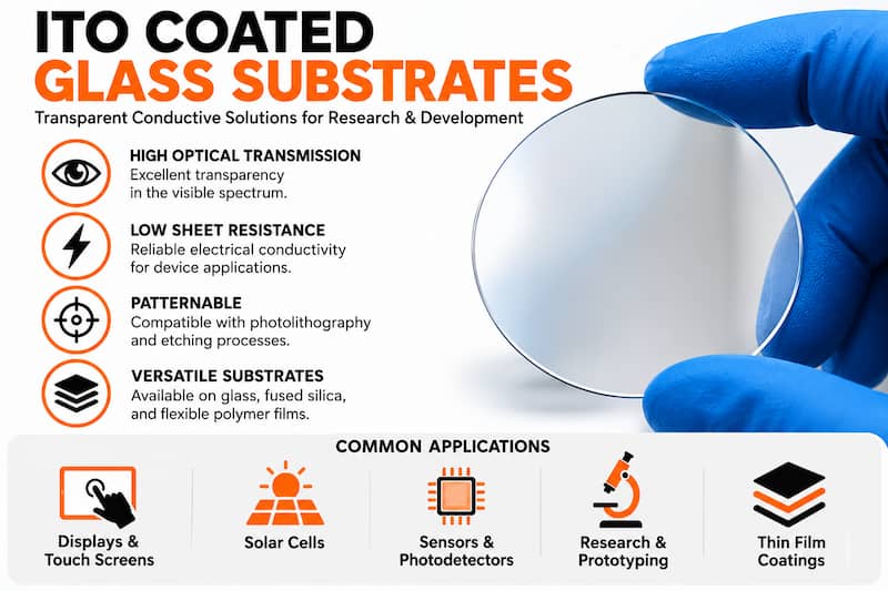
ITO-coated substrates are commonly used for:
Important ITO Substrate Specifications
ITO performance depends on more than substrate size. Researchers should
consider both the electrical properties of the coating and the optical and
mechanical properties of the underlying substrate.
Sheet Resistance
ITO sheet resistance is expressed in ohms per square (Ω/sq).
Lower sheet resistance generally indicates greater sheet conductance, but
electrical performance must be balanced against optical transmission and
other film requirements.
ITO Film Thickness
Film thickness influences resistance, optical transmission, interference
behavior, and processing characteristics. The optimum thickness therefore
depends on the intended device rather than on a single universal value.
Surface Roughness
Surface roughness can be especially important for nanoimprint lithography,
thin-film stacks, optical devices, organic electronics, and nanostructure
fabrication. Specify whether the roughness requirement applies to the
coated ITO surface, the uncoated substrate surface, or both.
Optical Transmission
Transmission depends on wavelength, ITO thickness, carrier concentration,
substrate material, surface condition, and deposition parameters. If your
application operates at a specific wavelength, request transmission data
for the appropriate coating and substrate combination.
ITO Coating and Patterning
Magnetron sputtering is widely used to deposit ITO thin
films because film thickness, composition, and electrical properties can be
controlled across relatively large substrates.
ITO can subsequently be patterned by techniques such as
photolithography followed by wet or dry etching.
Patterned deposition and lift-off may also be possible for compatible
processes. The appropriate method depends on feature size, film thickness,
substrate compatibility, resist system, and required edge definition.
ITO on Glass vs. ITO on Flexible Polymer
ITO can be deposited onto both rigid glass substrates and flexible polymer
films such as PET or PEN.
| Property |
ITO on Glass |
ITO on PET/PEN |
| Mechanical Form |
Rigid |
Flexible |
| Optical Flatness |
Can be very high depending on glass grade |
Generally lower than precision glass |
| Thermal Processing |
Usually tolerates higher temperatures |
Limited by polymer thermal stability |
| Typical Uses |
Displays, sensors, optics, lithography, photovoltaics |
Flexible electronics, sensors and transparent electrodes |
What Is Spin-Curve Testing?
A spin curve characterizes how the final thickness of a
spin-coated material changes with processing conditions, particularly
rotational speed. It is commonly generated for photoresists, polymers,
sol-gel coatings, and other liquid-deposited thin films.
How Spin-Curve Testing Works
-
Prepare the substrate.
Clean and dry the ITO-coated glass or other test substrate.
-
Dispense the coating.
Apply a controlled amount of resist, polymer, sol-gel, or other solution.
-
Spin the substrate.
Repeat the coating process at several rotational speeds while controlling
other variables such as dispense volume, acceleration, spin time,
temperature, and humidity.
-
Measure the resulting film.
Depending on the material, thickness can be measured using techniques
such as profilometry, ellipsometry, reflectometry, or interferometry.
-
Create the spin curve.
Plot measured film thickness against spin speed to establish an empirical
relationship for that particular coating process.
Many spin-coating systems exhibit an empirical relationship that can be
approximated as:
t = kω−n
where:
- t = final film thickness
- k = process-dependent constant
- ω = rotational speed
- n = experimentally determined exponent
The constants are not universal. They depend on properties such as
viscosity, solids concentration, solvent evaporation rate, spin time,
acceleration, environmental conditions, and interactions between the
coating and substrate.
Why Use ITO Glass for Thin-Film Research?
ITO-coated glass provides researchers with an optically transparent surface
that can simultaneously act as an electrical electrode. This combination is
useful when thin films must be deposited, electrically contacted, and
optically characterized through the same substrate.
Applications include photoresist development, organic and perovskite
devices, electrochemical structures, optical sensors, thin-film
photovoltaics, transparent heaters, and experimental display structures.
What to Specify When Ordering ITO Substrates
- Substrate material: glass, fused silica, PET, PEN, or other material
- Diameter or dimensions
- Substrate thickness
- Sheet resistance (Ω/sq)
- ITO film thickness
- Optical transmission requirements
- Surface roughness or flatness
- Coating on one or both sides
- Patterned or unpatterned ITO
- Pattern dimensions or mask requirements
- Quantity
ITO Coated Glass Wafers and Substrates
Indium tin oxide (ITO) is a transparent conductive oxide
commonly deposited onto glass, fused silica, and other substrates when a
combination of electrical conductivity and optical transparency
is required.
UniversityWafer supplies ITO-coated substrates for research involving
transparent electrodes, displays, sensors, photovoltaics, electro-optics,
nanoimprint lithography, and other thin-film devices. Important ordering
parameters include substrate material, dimensions, ITO thickness,
sheet resistance, optical transmission, surface roughness, and coating area.
ITO Coated Glass for Research
A postdoctoral researcher requested ITO-coated glass with the following general requirements:
Polished 4-inch glass substrates coated with ITO, including configurations
with sheet resistance below approximately 10 Ω/sq and below 7 Ω/sq.
The researcher also needed a relatively small quantity rather than a
production-volume order.
Reference #180192 for specifications and pricing.
ITO coatings can be supplied on different substrate sizes and thicknesses
depending on project requirements.
ITO Wafers for Nanoimprint Lithography
Surface quality can be especially important when ITO-coated substrates are
used for nanoimprint lithography, photolithography, optical
structures, or other processes involving nanoscale features.
A graduate researcher requested ITO-coated glass with extremely smooth
surfaces, targeting surface roughness below approximately 1 nm Ra for a
nanoimprint lithography experiment.
Reference #203125 for the original request. When surface
roughness is critical, specify whether the requirement applies to the
ITO-coated surface, the uncoated substrate surface, or both.
The final surface roughness depends on the substrate finish as well as the
deposited ITO film.
ITO Optical Transmission and Sheet Resistance
Two of the most important properties of an ITO coating are
sheet resistance, usually expressed in ohms per square
(Ω/sq), and optical transmission. These properties are
related to film thickness, carrier concentration, deposition conditions,
annealing, substrate material, and wavelength.
In general, increasing the electrical conductance of an ITO film can affect
its optical performance. For this reason, researchers should specify the
wavelength range and electrical requirements of the application rather than
selecting a coating from sheet resistance alone.
A researcher evaluating 50 mm × 50 mm and 100 mm × 100 mm ITO-coated
glass requested information about substrate type, dimensional tolerance,
edge coverage, and the optical transmission curve of a low-sheet-resistance
ITO coating.
Reference #209660. Transmission data should always be
associated with a specific coating thickness, substrate, and measurement
wavelength range.
What Is an ITO Thin Film?
Indium tin oxide is generally based on tin-doped indium oxide.
It is a heavily doped, typically n-type transparent conducting oxide.
Properly processed ITO films can combine relatively low electrical
resistance with high transmission through much of the visible spectrum.
ITO is usually deposited as a thin film rather than used as a bulk
structural material. Common deposition techniques include
magnetron sputtering, other physical vapor deposition
methods, and specialized chemical deposition processes.
Film properties can vary considerably with oxygen partial pressure,
substrate temperature, deposition power, film thickness, composition,
post-deposition annealing, and substrate surface condition.
How Can ITO Be Conductive and Transparent?
ITO combines these properties because its electronic structure permits
visible-light transmission while a high concentration of free electrons
provides electrical conductivity.
Optical Transparency
ITO has a wide optical band gap, so properly prepared thin films can
transmit a large fraction of visible light. Optical behavior is not
determined by band gap alone, however. Film thickness, free-carrier
absorption, defects, surface roughness, and interference effects also
influence measured transmission.
Electrical Conductivity
Tin incorporation and oxygen-related defects can contribute free electrons,
producing a high carrier concentration and relatively low resistivity.
ITO is therefore often described as a
degenerate n-type semiconductor.
Transparency-Conductivity Trade-Off
Increasing carrier concentration or coating thickness can decrease sheet
resistance, but it can also increase optical absorption and reflection,
particularly outside portions of the visible spectrum. Device designers
therefore optimize the film for the required combination of transmission
and electrical conductivity.
Common ITO Substrate Applications
Touchscreens and Displays
ITO is widely used as a transparent electrode in display and touch-interface
technologies because patterned conductive regions can be formed while
maintaining substantial visible-light transmission.
Solar Cells and Photovoltaic Research
In photovoltaic structures, ITO can function as a
transparent conducting electrode, allowing light to reach
the absorber while providing an electrically conductive contact.
Sensors and Electro-Optical Devices
ITO-coated glass can be used in optical sensors, electrochemical devices,
heaters, transparent electrodes, photodetector structures, and
research devices requiring simultaneous electrical access and optical
transmission.
Thin-Film and Nanofabrication Research
ITO substrates are also useful for lithography, thin-film deposition,
nanostructure fabrication, microscopy experiments, and electrically active
optical surfaces.
Typical ITO Glass Sizes
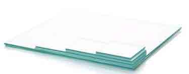
ITO-coated substrates can be supplied as wafers, squares, rectangles,
slides, and larger glass panels. Examples include:
- 25 mm × 25 mm
- 25 mm × 75 mm
- 50 mm × 50 mm
- 50 mm × 75 mm
- 100 mm × 100 mm
- 150 mm × 150 mm
- Custom wafer diameters and rectangular dimensions
Example ITO Coated Glass Configurations
| Item |
Size |
Thickness |
Example Specification |
|
2276
|
25 mm × 25 mm |
0.7 or 1.1 mm |
ITO-coated glass, approximately 15–20 Ω/sq |
|
2272
|
75 mm × 25 mm |
0.7 or 1.1 mm |
ITO-coated glass, approximately 5–20 Ω/sq |
|
2530
|
50 mm × 50 mm |
0.7 mm |
ITO-coated boro-aluminosilicate glass |
|
2288
|
150 mm × 150 mm |
0.7 or 1.1 mm |
ITO-coated polished glass, approximately 10 Ω/sq |
Availability and specifications can change. Confirm sheet resistance,
ITO thickness, substrate type, dimensions, tolerances, and coating coverage
when requesting a quote.
ITO Coated PET Film
ITO can also be deposited onto transparent polymer films such as
polyethylene terephthalate (PET). Compared with glass,
PET provides flexibility and lower weight, but its lower thermal stability
places additional constraints on deposition and post-deposition processing.
ITO-coated PET can be useful for flexible electronics, transparent
electrodes, sensors, touch interfaces, and experimental optoelectronic
devices. Important specifications include sheet resistance, visible
transmission, PET thickness, haze, surface roughness, coating adhesion,
and allowable processing temperature.
How Is ITO Patterned?
ITO films can be patterned using either subtractive etching or
deposition-based patterning. The best process depends on ITO thickness,
substrate material, feature size, resist compatibility, and required
sidewall quality.
Wet Chemical Etching
Acid-based wet etchants are commonly used for relatively simple ITO
patterning. Wet etching is generally inexpensive and suitable for larger
features, although lateral etching can limit dimensional control for very
small structures.
Dry Etching
Plasma-based processes such as reactive ion etching can provide improved
feature control for micro- and nanoscale patterns. Actual etch chemistry
and selectivity depend strongly on the ITO film, resist or hard mask,
substrate, and equipment.
Lift-Off
In some fabrication flows, patterned deposition and lift-off can be used
instead of etching. Whether this approach is practical depends on the ITO
deposition method, substrate temperature, resist profile, and required
feature geometry.
Choosing an ITO Coated Substrate
When requesting an ITO-coated substrate, specify as many of the following
parameters as possible:
- Substrate: glass, fused silica, PET, or other material
- Shape and size: wafer, square, rectangle, slide, or custom dimensions
- Substrate thickness
- ITO sheet resistance: Ω/sq
- ITO thickness
- Required optical transmission and wavelength range
- Surface roughness
- Single-side or double-side coating
- Edge exclusion or full-area coating requirement
- Patterning or additional thin-film requirements
Defining these parameters helps match the ITO coating and substrate to the
electrical, optical, and fabrication requirements of your research.
Shop ITO Coated Glass and Check Availability »
Related Transparent Conductive Substrates
