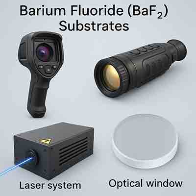
BaF2 Substrates Used For Optical Structure
A doctoral candidate in applied physics requested a quote for the following.
I was wondering if I could get a quotation for BaF2 wafers, 1-inch and 2-inch diameter, both sides polished.
Quantity: 5
Diameter: 2 inches
Doping: No
Both sides polished.
Thickness: between 200 and 500 microns
I'm gonna use it as substrate for optical structures, so I don't care about the other specs. I just want it to be transparent between 3 and 10 microns.
Reference #105906 for specs and pricing.
Get Your FAST! Or, Buy Online and Start Researching Today!
What are Barium Fluoride (BaF2) Substrates and How Are They Used in Semiconductors?
Barium Fluoride Substrates (BaF₂) are single-crystal substrates made of barium fluoride, a compound with a cubic fluorite crystal structure. These substrates are primarily used in specialized applications due to their unique properties, which include a wide bandgap, high optical transparency, and low refractive index.
Properties of Barium Fluoride
- Crystal Structure: Cubic (fluorite structure).
- Bandgap: Wide bandgap (~10–11 eV), making it suitable for UV and extreme UV applications.

- Transparency: High transparency across a broad wavelength range (UV to IR, approximately 150 nm to 12 µm).
- Thermal Stability: Stable under moderate temperatures but limited by its relatively low melting point (~1360°C).
- Low Refractive Index: ~1.46, similar to that of fused silica.
- Chemical Resistance: Resistant to many chemicals but can degrade in water or humid environments due to partial solubility.
Applications in Semiconductors
Barium fluoride substrates are used in specialized semiconductor and optoelectronic applications, particularly where their optical and electrical properties are advantageous. Common uses include:
-
Optoelectronics and Photonics:
- Fabrication of UV-transparent windows and coatings.
- Substrates for optical devices in extreme UV applications.
- Thin-Film Epitaxy:
- Barium fluoride substrates can act as templates for the epitaxial growth of other materials, particularly those with similar lattice parameters, such as certain II-VI semiconductors (e.g., CdTe, PbTe).
- Their lattice match facilitates the growth of high-quality crystalline films, often used in IR detectors and photovoltaic devices.
- Microelectronics:
- Though less common, they are used in niche applications where their insulating and wide bandgap properties are beneficial, such as high-frequency or high-temperature electronic devices.
- Radiation Detection:
- BaF₂ is used in scintillation detectors because of its luminescent properties under high-energy radiation, which also makes it valuable in semiconductor radiation sensing technologies.
Advantages and Limitations
-
Advantages:
- Excellent optical clarity over a broad spectrum.
- High lattice compatibility with certain materials for thin-film growth.
- Wide bandgap supports high-temperature and high-energy applications.
- Limitations:
- Susceptible to degradation in humid environments.
- Mechanically softer than many other substrates, making it prone to scratches and wear.
- Relatively low thermal conductivity compared to other semiconductor substrates like silicon or sapphire.

Barium Flouride Based Devices
Use Cases in Comparison to Other Substrates
Barium fluoride is not as widely used as silicon or sapphire in mainstream semiconductor applications due to its specific properties and limitations. However, for highly specialized applications—such as UV optics, IR devices, or specific thin-film semiconductors—it offers unmatched advantages in terms of lattice matching and optical transparency.
Would you like detailed information on specific applications or growth techniques for BaF₂ substrates?


