
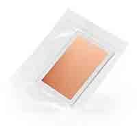
What are the substrate requirements for this process? “Monolayer Graphene on Your Substrate?”
Need Graphene‑Coated Substrates?
CVD monolayer graphene on SiO2/Si, Quartz, PET, Cu — or on your substrate. Sizes up to 4" dia. Fast lead times.
- Metal‑free transfer available
- Custom cuts & sheet sizes
- Target specs: ≤120 °C bake, acetone/IPA/H2O compatible
- Reference inquiries welcome (e.g., #198286, #259474)
Trusted by researchers & engineers at universities and industry worldwide.
Graphene for Sale - Products for Researchers
UniversityWafer, Inc. is a leading Graphene Supplier. Graphene has shown to have superior properties that range from mechanical to electronic. Some scientists suggest that graphene's full potential is in unique applications that are designed to work with graphene instead of replacing a traditional material such as silicon.
What Substrates Can Graphene Be Deposited On?
A postdoc asked the following:
We can deposit onto most of the substrates. The maximum size is 4 inches diameter and the substrate must resist acetone, IPA, distilled water and a thermal treatment (around 120ºC).
Reference #198286 for specs and pricing.
Get Your Graphene Quote FAST! Or, Buy Online and Start Researching Today!
The Field of Nanotechnologies
An undergraduate requested help in what he should research:
I am interested in the substance of graphene and would like to learn as much as possible about it so that I can make an informed decision about a move into the field of nanotechnologies. In doing preliminary research, the potential benefits seem to greatly outweigh the current costs of research and development. Graphene holds properties that are unmatched and its potential uses are seemingly endless. It is my goal to learn about the field in general, however, I do not have a technical background. With a history and education degree, my skill set is geared towards analyzing, presenting, and implementing. A good place for me to begin understanding both the graphene market and future is sales. I would be greatly appreciative for any and all information that you might be able to provide me relating to current or anticipated markets and products, as well as other information sources that might be helpful to gaining a better understanding. I realize this request may seem unique, however, I would like to see if this substance is as outstanding as I have been hearing.
Reference #210327 for our answer.
Graphene Keywords
- graphene sheets
- graphene devices
- graphene depends
- graphene buffer
- exfoliated graphene
- dielectric layers
- electron density
- different graphene
- graphene plane
- electronic properties
- hexagonal boron
- absorption coefficient
- original graphene
- hole mobility
- experimental values
Graphene Material Discoveries
Researching two-dimensional materials and their heterostructures, offers the potential for amazing scientific discoveries and the promise of real-world uses that does not require new tooling.
Graphene is lightweight, stiff, and strong. In fact, it’s one of the strongest materials known to man. Graphene properties have many uses including making incredibly strong composite materials such as mixing graphene with plastics that have incredible strength per unit of mass.
Graphene Coating on Silicon Wafers
We are investigating the use of graphene coating on silicon wafers to facilitate the absorption and conversion of light into photovoltaics in the next generation of silicon solar cells. Ultimately, the efficiency of silicon PV cells could be up to 1300%. In order to coat the graphene coatings, they can be dissolved from the substrate with the help of a thin film of water.
Five Cool Graphene Uses Video
One of the most fascinating graphene applications is its use as a bionic implant. In March 2012, the journal Nature featured a study that predicted bionic implants using the material. The study's lead author, Aravind Vijaraghavan, said graphene has the potential to interact with biological systems and talk to cells. While this has not yet been commercialized, this application is already showing promise in many fields.
The materials amazing physical properties mean that they can be combined with other elements. Researchers are already experimenting with graphene in a variety of applications, from antennas to saltwater filters. DNA-sequencing devices are just a few of the technologies using the material. Samsung is investing hundreds of millions of dollars in research into the material. In the near future, we may even see the first cellular phone made from graphene.
Graphene can also be used to create flexible touch-screen displays, rigid metal housing, and energy cells. With its unique structure, graphene can conduct electrical current and heat better than copper and diamond. In addition, it is transparent, which means that it can be used to see through objects. With these amazing properties, graphene is on the verge of revolutionizing many industries. And since there are so many applications for this material, it's only going to continue to grow.
Silicon Wafers for Graphene-Based Nanomaterials Research
Scientists at Northwestern University have used the following Silicon Wafer Item for their following research:
X-ray photoelectron spectroscopy (XPS) was gathered in the Keck II/NUANCE facility at Northwestern University using a Thermo Scientific ESCALAB 250Xi (Al Kα radiation, hν = 1486.6 eV) (Thermo Fisher Scientific Inc., West Palm Beach, FL) equipped with an electron flood gun. Samples for XPS analysis were prepared via LB deposition of GO and GO-PVA onto Si wafers (Item #785, 100 mm diameter, p-type, B-doped, single side polished) purchased from University Wafer, Inc. (Boston, MA). XPS data was obtained from three different locations on the surface of each sample, and was analyzed using Thermo Scientific Avantage Data System software (version 5.923), with a Smart background subtracted prior to peak deconvolution and integration.
What Substrates are used for Exfoliating 2D Materials?
A graduate student requested help with the following:
I wanted to buy 150 mm Si wafers, but confused about the grade specification. Could you please detail me about the prime, mech, test grade wafers. Is it about surface flatness? We want to use the wafers for exfoliating 2D materials, namely, Graphene, Boron Nitride, etc. However, we aren't fabricating any device on theses wafers. For exfoliation, we want the surface to be clean and flat.
We wanted to buy Si wafer with following specs:
Silicon 150mm, Res>= 100 ohm-cm, 625-675 thickness, SSP PRIME w/285nm DRY Thermal Oxide
Qty 10
Could you send me a quote for these spec?
Reference #225883 for specs and pricing
What Graphene Coated Silicon Wafers are Used for Neutron Reflectivity Experiments?
A Post-doctoral Research Associate requested the following quote:
Hello, I will doing a neutron reflectivity experiment this month and would like some graphene coated silicon wafers : quantity 3 The wafers need to be round 4 inch (10 cm) in diameter and ideally 10 mm thick. One side (the side the graphene will be deposited on) will need to be polished to a target rms roughness 0.1 nm (1 Angstrom). The silicon will also need to be n-type doped (phosphorous) with either 110 or 111 Orientation.
I would love a quote for the silicon also! Could you please also provide details of the Si in terms of surface roughness and if it satisfies the requirements I mentioned in the original request?
10 mm thick is right. 4 inches in diameter.
Reflectivity is a temperamental and expensive game unfortunately and thicker substrates actually reduce noise in the measurements. The instrument is called 'Spatz' has a 3 sample changer. Hence why I want 3 substrates.
The substrates should be mostly pure silicon. The surface oxide layer on the polished side should only be a few angstroms.
Reference #258596 for specs and pricing.
What is The Sheet Resistance of Graphene on PET?
An Assistant Professor Electronic Engineering Dept asked the following:
Question:
Can you provide the sheet resistance of graphene on PET samples, large area especially?
2 questions:
- is 1cmx 1 cm the largest size? Can you provide 5cm x 5cm?
- Is it possible to have lower sheet resistance (around 100 Ohm/sq max)?
UniversityWafer, Inc. Answer:
The Sheet Resistance on PET is 580±50 Ohms/sq (1cm x1cm)
We can make custom size substrates, in this case 5cm2.
Monolayer Graphene M on PET
G/PET/Custom/M-25
Monolayer Graphene (5 cm x 5 cm) on PET
Reference #259474 for specs and pricing.
What is the weight of a Graphene sheet?
A single layer of graphene, which is essentially a two-dimensional material, weighs very little due to its extreme thinness. Graphene is a single layer of carbon atoms arranged in a hexagonal lattice, with a thickness of only one atom.
To estimate the weight of a graphene sheet, we can consider the area of the sheet and the density of graphene. Graphene has a density of about 0.77 mg/m². This means that a one square meter sheet of graphene would weigh about 0.77 milligrams.
For example, if you have a graphene sheet that is 1 square meter in size, it would weigh approximately 0.77 milligrams. For different sizes, you can scale this weight accordingly based on the area of the sheet. However, it's important to note that this is a theoretical calculation and actual weights may vary slightly due to imperfections or additional layers in practical graphene sheets.
What Catalyst Substrates Can Be Used for Graphene and Carbon Nanotubes?
A corporate researcher requested the following:
I have an urgent requirement for the following wafers .
- 500 nm Cu deposited on Si wafer with 100nm Sio2. Of size 4”
- 500 nm Ni deposited on Si wafer with 100nm Sio2. Of size 4”
- 5nm Ni deposited on Si wafer with 100 nm sio2 + 70 nm TiN of size 4”
- 1nm Fe deposited on Si wafer with 100 nm Sio2+ 70 nm TiN of size 4”
Initially if we would get a quote for some sample wafers of each type which we can use to test our processes for graphene and Carbon Nanotubes. Alternatively if you have experience in supplying catalyst wafers for Graphene and Carbon nanotubes, please send me some data and we will consider a batch order.
I have been having discussion regarding the wafer request I had sent you in order to proceed forward. What we are trying to do is to grow nanotubes and graphene on those substrates and from our experience we find that the process is highly dependant on the source of the catalyst wafers. In order to be confident both from our side that we can offer this to our clients as well as to ensure that this will be a recurring order we were wondering if it would be possible to get one or two wafers of each just for us to test and ensure that they work for us. We will then quickly run our processes on them and follow it up with a larger order.
Reference #198099 for answers, specs and pricing.
What Graphene is used Modelling and Characterization of Photonic Devices?
A PhD student studying nanophotonics, particularly, nanoscale subwavelength optical elements and systems, nanoplasmonics, applications in UV lasers, high efficiency LEDs and solar cells, and ultra-sensitive biosensing, asked the following question.
I am very interested in the Postdoc position in nanophotonics as my PhD project is about modelling and characterization of graphene photonic devices, and my MSc project is about optical sensing. Could you give me more information involving this position? Thanks a lot for your time and information!
Reference #212328 for answer.
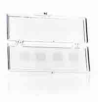
Can Graphene Be Transferred Onto a Clean Semiconductor Surface?
A Ph.D and Fellow SPIE researching Quantum Semiconductors requested help with the following project.
Could you please get me more information about:
- Monolayer Graphene on your substrate? What surface area? What substrate? Graphene or graphene oxide?
- Monolayer Graphene on SiO2/Si (1 inch x 1 inch)
Could this graphene be transferred to a clean semiconductor surface?
UniversityWafer, Inc. Answered:
We can transfer Graphene films, not graphene oxide, onto many different substrates, please find attached a short questionnaire regarding your substrates, which we would be grateful if you could complete, in order to know if we can transfer graphene on them. The minimum sheet size we can transfer is 3 mm diameter up to 4 inches diameter wafer.
Regarding the graphene on silicon, I regret to tell you that you can not transfer this graphene on to a semiconductor surface. Anyway, we can transfer our graphene on to your semiconductor. This would be the Monolayer Graphene on Your Substrate. To make a quote we would need you to complete our questionnaire and to know the graphene size you want to transfer.
Reference #216138 for questionnaire.
What is Graphene? Let's Explore Its Mechanical Properties and Reversible Chemistry
What is Graphene? Let us explore its mechanical properties and reversible chemistry. Graphene is the most  abundant natural substance in the world. Its electronic structure makes it one of the most flexible materials. It can be used for electronics, medical implants, and solar panels, as well as in many other applications. The reversible chemistry of Graphene makes it one of the most promising materials for future energy technologies.
Graphene
Graphene is a material made of carbon atoms. In its simplest form, graphene is just one layer. But it's capable of many more things than that. It's extremely strong and is more than a thousand times stronger than copper. Its unique structure allows electrons to flow through the material unhindered. Graphene has a highly pronounced field effect, which allows scientists to control its conductivity.
It's also extremely thin and lightweight, making it ideal for heat-spreading solutions. Graphene-based thermal foils can make LED lights last longer and are becoming increasingly popular in smartphones. Huawei has even begun using graphene-based thermal film on its phones. In addition to being strong and lightweight, graphene also disperses heat more efficiently, so it's a great choice for mobile devices.

The carbon atoms that make up graphene are connected together using a honeycomb-like structure. Each sublattice is comprised of three atoms; the resulting honeycomb structure mimics the internal angular momentum of subatomic particles. Graphene electrons have the same role as electrons and positrons in quantum electrodynamics. However, their velocity is fractional to the speed of light.
Graphene's electronic properties are dictated by its pi orbitals, which form a valance band and conduction band. These two bands are crucial to understanding graphene's properties. These properties are important for many applications, from making electronics to manufacturing new products. The next step in graphene's development is the manufacture of new products. Once it is ready for the mass market, graphene may even replace some existing materials.
Graphene is a great electrical conductor and has countless uses. It's the basis of solar panels, LCDs and touchscreens. Its strength, transparency, and electrical conductivity make graphene a fantastic material for electronics. Its many applications are virtually limitless, and the potential is truly staggering. If you've ever tried to make graphene, you've probably seen it. Just look at the applications.
Graphyne
Graphyne is a thermoelectric material that has excellent mechanical properties. However, its properties may be altered by the adsorption of other atoms. Graphyne can prevent mechanical failure caused by thermal expansion or contraction. In a recent study, researchers discovered that a few-layer graphyne exhibits fold edge structure. A single flake of graphyne has a height of 9 nm.
The synthesis of graphene on a copper substrate was successful, as it is composed mainly of elemental carbon. Using energy dispersive X-ray spectroscopy, graphdiyne on copper foil can be distinguished by its characteristic carbon-carbon bonds. The resulting polymer displays acetylenic and aromatic rings. Graphene is a promising material for electronics. However, its production is highly expensive and requires complex equipment.
While one study reported the fabrication of a single-layer graphyne, there is no other study that shows the same results. In contrast, the symmetry of a six-layer graphyne makes it suitable for electrical grating. This property could lead to the development of faster transistors and a variety of other electronic components. In the future, Graphyne may even become an inexpensive material for solar cells.
The mechanical properties of graphene are controlled by strain rate and temperature. Both tensile strength and Young's modulus will decrease significantly when cracks occur in a material. The crack-resistant properties of b-graphyne might be attributed to its triangular structure. If it is possible to create a high-strength polymer, this material will be a useful material for electronic applications.
Graphene's Reversible Chemistry
Graphene's reversibility has led to several interesting discoveries. Among the discoveries that have occurred in recent years are those that reveal how graphene's chemical properties can be controlled. The reversible nature of graphene has enabled researchers to develop nano-scale devices that are able to mimic many of our everyday objects. This property, as well as its unique properties, are the basis for further research.
Graphene can conduct electricity at zero carrier concentration. This property is achieved by the fact that the electrons do not localize or slow down. They simply move around the carbon atoms, interacting with the periodic potential of the graphene honeycomb lattice to produce new quasiparticles. These new particles are massless Dirac fermions, which travel much faster than electrons in other semiconductors.
In addition, graphene can be dissolved in solvents or folded. When dissolved, a single layer of graphene oxide can lose as much as 20% of its carboxylic functionality. As a result, this material is highly thermally unstable. In this case, the chemical reaction between thionyl chloride and graphene oxide can lead to the formation of aromatic and aliphatic amides.
Graphene's reversibility also allows researchers to make a graphene-based device without sacrificing performance. Researchers are studying graphene's reversible chemistry to create high-performing devices that can be worn by humans. The material is also capable of producing a range of next-generation technologies such as ultrasensitive sensors, wearable electronics, and multifunctional coatings and composites. Since its discovery in 2004, graphene research has grown into a vast field with more than 10,000 publications published every year.
What are Graphene's Mechanical Properties?
Graphene is a sheet of carbon atoms, each one atom thick. The atoms in graphene are arranged in a layer with two p-state bands, and these orbitals are responsible for the material's incredible mechanical properties. These properties make graphene the hardest material known to science, and the researchers believe that further exploration of this material will yield many additional applications.
Graphene is so thin that it looks 2D, but it is actually three-dimensional. Unlike other 2D materials, graphene's electronic orbitals are perpendicular to the atomic plane. Because of this, graphene exhibits mechanical properties similar to those of graphite. A recent paper published in Physical Review Letters describes the testing of graphene's mechanical properties.
Graphene's unique structure makes it an ideal host material for electrodes. The structural defects of graphene prevent dendrites, which are branch-like filaments that develop on the electrodes. These dendrites can cause fires and electrical shorts. This material's high surface area means that it can absorb more impact than a typical helmet. Furthermore, graphene's heat dissipation properties make it a better choice for fuel cell catalysts.
As graphene's mechanical properties have been studied, researchers have found a way to detect the defects in the material. Graphene's surface is smooth, so a sand-like grain will have a smooth appearance. Graphene also has excellent optical properties, which makes it a great candidate for sensors and other applications. This material may soon become a common commodity, such as batteries and computer displays.
Although graphene's mechanical properties are excellent, they are not sufficient for flexible electronic devices. Graphene has some defects that can cause it to fracture and break, causing damage to the resultant device. There are effective methods of observing these defects, such as transmission electron microscopy, scanning tunneling microscopy, and atomic force microscopy. Recent research has addressed these issues, including using a process called defect healing.
Graphene's Potential as a Semiconductor
Graphene's high conductivity, thermal stability, and strength make it an ideal candidate for a wide range of applications, including electrical and biomedical ones. The ability to change the behaviour of cells inside the body could prove valuable in biomedical applications, including drug delivery. Today, plastic packaging allows water molecules to enter the product, reducing its shelf-life. Graphene, however, can reduce the absorption of water by millions of times. As such, it can be used as a water-repellent floor, as well as on glass surfaces, textiles, and ship hulls. Full market penetration will probably come within five to ten years.
One of the most fascinating features of graphene is its ability to function as a semiconductor at room temperature. Its zero-gap structure allows the conduction and valence bands to meet at Dirac points. Nanoribbons of graphene are known as graphene, and they are zig-zag in nature. However, they have a non-metal band, which means they are still conductors.
Although graphene is currently available for fabrication, it has to be integrated into the semiconductor industry. It will require a detailed understanding of its properties, as well as a method to implement it in a fabrication environment. Because the semiconductor industry is commercial, any technical challenges must be overcome without disrupting the entire manufacturing process. In addition, graphene must offer a significant performance advantage. However, it is important to note that research in this field is not yet complete.
The ability of graphene to act as an actuator is a key aspect of this material's potential as a semiconductor. The ability to change the dimensions of a material has many applications, including artificial muscles, microelectromechanical systems, and biomimetic nanorobots. Nanoribbons of graphene can be used to create actuators in such systems. The technology is rapidly evolving and a breakthrough will be made soon.
Video: Graphene 101Graphene Materials Inventory
Below are just some of the Graphene materials that we have in stock.
Please let us know what you need.
Monolayer Graphene on SiO2/Silicon (Si)
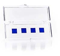 UniversityWafer, Inc’s monolayer graphene (SIO-2-4) substrates is produced by the Chemical Vapor Deposition (CVD) process a two-dimensional (2D) material by a wet transfer to a circular wafer. The CVD method has been used to grow a single layer of graphene. We transfer the Copper (Cu) onto the silicon’s wafer surface using the wet transfer process.
Advantages of Monolayer Graphene on SiO2 Silicon
Graphene is a material with unique optical properties. It is a single layer of atoms that absorbs 2.3% of incident light. When the light strikes the material, it generates electrons and holes. This property makes it different from traditional semiconductors. Its thermal conductivity is high, too. The following are some advantages of this material. It is a promising material for energy storage.
The main advantage of monolayer graphene films is that they are metal-free. This is important for the 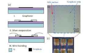 development of high-performance graphene-based devices. Current CVD processes suffer from low structural uniformity, poor growth rate, and negligible catalytic activity of dielectric substrates. In this context, a new water-assisted chemical vapor deposition (VACVD) process is developed. Using water, this method is optimized for the growth of monolayer graphene. Furthermore, it lowers the kinetic barrier of the material, enabling rapid and preferential formation of graphene films.
The production of large-format monolayer graphs is possible through the CVD process and fixing a multilayer graphene film onto a TI adhesive layer. Then, the resulting double bilayer graphene is etched away from the nickel layer, leaving a thin layer of graphene directly on the silicon oxide. The process requires a temperature of 1000degC.
The high-quality graphene products can be made using multiple CVD processes. They can reach 90% coverage and are suitable for product R&D applications. They are also very cheap and can be fabricated using commercial equipment. One of the advantages of monolayer graphene on silicon is its low sheet resistance. The material is transparent, making it an ideal conductor for electronic devices. Moreover, it is compatible with all types of substrates.
For high-performance graphene devices, metal-free growth of monolayer graphene films is necessary. Existing CVD processes, however, are limited by their lack of structural uniformity, slow growth rate, and low catalytic activity. A water-assisted CVD process has overcome these limitations by using water as an additional catalyst. It allows the formation of highly-uniform monolayer graphene films in a much shorter time.
Graphene on silicon is a very dense material that offers high-light transmittance. It is the perfect material for all kinds of applications, including solar cells, battery cells, and transistors. It is highly transparent and has very low density. It is a versatile material that can be used in many fields. This material has many applications and has tremendous potential. It has been demonstrated in a variety of fields, including electrical and optical communications.
A new water-assisted CVD process has the potential to grow monolayer graphene films. This process is a high-temperature technique, and the use of water allows the use of low-temperature synthesizers. Besides, it can be used to create transparent conductors and other electronic devices. Although a new water-assisted CVD process can be used for high-performance device fabrication, it is not yet commercially available.
A CVD process is the most popular way to produce single-layer graphene. This method uses methane, but other carbon-containing compounds can be used. The carbon source is then deposited on a substrate, such as copper foil. This process can also be used to deposit graphene on non-conductive substrates. It is useful for a variety of product R&D applications, including battery manufacturing.
A CVD process that produces monolayer graphene is the most commonly used method for growing monolayer graphene. It requires a gas mixture of methane and oxygen to form monolayer graphene. The gas is then heated to 800-1000degC and the carbon source is deposited on the substrate. In addition, a water-assisted process is preferred for monolayer graphene growth, as it lowers the kinetic barrier and allows a greater extent of morphology and structural uniformity.
In contrast to the traditional CVD process, a single layer of graphene with copper catalyst was grown on quartz substrates. After transfer to the silicon, the graphene films were transferred to Si-SIO-2 via a copper transfer method. The graphene layer was then transferred to a silicon lid by VTD. After this, it was analyzed by SEM to determine the quality of the deposited film.
Monolayer Graphene on Your (Any) Substrate
 From glass to silicon to glass, we can deposit graphene monolayer onto it using the Chemical Vapor Deposition (CVD).
Suspended Monolayer Graphene on Cavities
Graphene in electronics have superior properties to traditional materials. Graphene will be light and stiff. Suspended graphene membranes have can be used optomechanical systems including NEMs. Suspended graphene nanocavities are driven by two horizontal Fabry-Perot cavities and one vertical Fabry-Perot cavity to exploit the standing wave properties of plasmonic resonance.
Suspended Monolayer Graphene on Cavities
Graphene on cavities was first introduced by Graphenea, a company that acts as a provider of graphene. The company has three patent applications and has developed a semi-dry transfer process in which a thin film of a single-layer graphene is placed over holes of up to 500 micrometers in diameter. The research has been successful, and it has led to further advancements in the field. The technology has many potential applications for optical, electrical, and mechanical applications.
Graphenea uses a proprietary PECVD process to grow graphene films on a quartz substrate. They  analyze the surface boundary conditions on the Mg samples deposited in molten quartz, as well as the complex refractive index and electrical conductivity of these materials. They have also shared their publications with world-leading graphene NEMS research groups, which make the materials more accessible to industrial use.
Graphenea's suspension monolayer graphene on a cavity material is a promising material for nanoelectromechanical systems (NEMS). These small devices require highly sensitive membranes that are extremely rigid and lightweight. The high Young's modulus and low temperature properties of the materials make them ideal candidates for microsupercapacitors. If you have ever wondered about the performance of such devices, you can now find out how it works.
The new material combines the benefits of conventional carbon and other materials. These new materials form two-dimensional sheets, which are more stable than single-layer graphene. They are conductive and exhibit varying forms of spin ordering. The researchers tested the new material's ability to control electricity with a perpendicular electric field. This new material is the perfect solution for applications in biomedical and medical research.
The new technology has the potential to revolutionize the world of medical devices. Unlike conventional medical devices, monolayer graphene is flexible and thin enough to allow for multiple applications. In addition, its properties also make it an excellent material for the pharmaceutical industry. If you're looking for high-quality, monolayer graphene is a great material for any device that requires electrical properties.
Graphenea has expanded its product line by adding Suspended Monolayer Graphenene on Cavities. These systems are nanoelectromechanical systems (NEMS), which are smaller cousins of MEMS. They are based on tiny, vibrating membranes that can be highly sensitive to small forces. These membranes need to be light and rigid and have a high Young's modulus to be effective.
Graphenea has expanded its product range by adding Suspended Monolayer Graphenene on Cavities. The company also aims to create new products for medical devices. Moreover, this technology can be incorporated into other products. The research will allow scientists to create a new type of device. This technology is an ideal material for use in different fields. It is used in a variety of applications such as sensors, semiconductors, and batteries.
Graphenea's technology is also useful for medical applications. These devices are more durable than MEMS and can be used as implantables. Unlike other materials, these materials are flexible, lightweight, and have high Young's modulus. Furthermore, they can be easily manufactured and shipped. There are no limitations to the potential applications of this new technology. Its use in medical devices is endless.
Graphenea's new technology allows scientists to use graphene as a semiconductor. Its sensitivity is superior to silicon-based MEMS. This material is suitable for a variety of applications. The high-resolution image will allow the semiconductor to be sensitive to electrical signals. Further, the device will be resistant to electromagnetic interference. Besides, the Graphene on the Cavities is suitable for many industrial applications.
Graphene oxide is a promising candidate for producing graphene. It contains flakes and monolayers of graphene. Its water platelets interact with the flakes, which makes it hydrophilic. Its low weight also improves the material's functionality. Moreover, it is a good candidate for industrial applications. These nanoelectromechanical devices are light-weight, and can be made into complex shapes.
Monolayer Graphene on Copper (Cu)
Growing monolayer graphene on Copper (Cu) thin films or Silicon (Si) Wafers works great for the production of massive direct graphene components. Researchers have demonstrated metal-based peeling processing the transfer of monolayers of graphene structures onto copper foil without destroying the base wafer.
Why copper foil? Cu is used for CVD growth because it enables production of large area single-layer graphene.
Monolayer Graphene on Cu (100mm)

Monolayer Graphene on Copper (Cu) (25.4mm x 25.4mm)
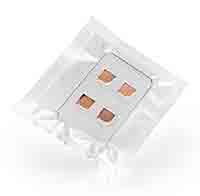
Monolayer Graphene on Cu (12mm Dia) Pack 4 Units
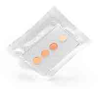
Monolayer Graphene on Cu (10mm x 10mm) Pack 4 Units
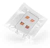
Monolayer Graphene on Cu with PMMA Coating (10 mm x 10 mm) - Pack 4 units
Monolayer Graphene on Cu with PMMA Coating (25.4mm x 25.4mm)
Monolayer Graphene on Cu with PMMA Coating (12 mm Circular) - Pack 4 units

Trilayer Graphene on SiO2/Silicon
 High-quality and uniform graphene films are applied to dielectric substrates to realize large-scale applications of graphene in electronics. The results here make off-axis substrates (Silicon Carbide SiC 0001 ) a good candidate for large-area trilayer graphene producing with favorable amber-splitting.
Graphene Oxide
Graphene oxide is one of the most popular 2D materials available and a fascinating nanomaterial that is huge. It is a widely dispersed solution that is bound to aqueous solvents and has useful properties and a wide range of applications in electronics, sensors and optics. Groups of water molecules move through hydrophilic solutions in this way. This forces flakes to form the outer layers of the fibre pack, creating a kind of skin.
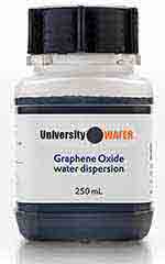
Graphene Oxide (4 mg/mL, Water Dispersion 5000 mL)
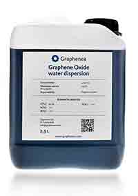
Graphene Oxide (4mg/mL, Water Dispersion 1000ML)

Graphene Oxide (4mg/mL, Water Dispersion 2500ML)
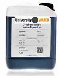
Graphene Oxide (0.5 mg/mL, Water Dispersion 250mL)
 Among other materials in the graphene family, graphene oxide (GO) and its reduced form (reduced graphene oxide or RGO) are of particular interest due to their high surface area, solubility in a variety of solvents, including water and aqueous solutions, and a variety of surface functionalization options for biomedical applications
Reduced Graphene Oxide (1 Gram)
 The reduction of graphene oxide (simultaneous peeling or reduction of graphite oxide) is considered the most promising for the large-scale production of graphene and is referred to as reduced graphene oxide or RGO. RGO is a form of graphene with similar properties to graphene, but with good conductor properties. There are several ways to reduce RGO that are inexpensive and simple. It is popular and attractive as an effective and cost-effective method for those who want to manufacture graphene-related materials such as RGO. The reduction of graphene oxide has proven to be of high quality, as it is practically identical to untouched graphene.
A partial reduction can be achieved by treating suspended graphene oxide with Hydrozine Hydrazine for 24 hours at 100 degrees Celsius, by exposing it for a few seconds to hydrogen plasma or by exposing graphene oxide to strong light pulses like xenon flashes. Thermal reduction produces a higher degree of reduction than chemical processes, which leads to higher electrical conductivity. The RGO with strong reduction contains residual oxygen and structural defects caused by chemical oxidation and synthesis of the reducing agents and can be synthesized from inorganic substances such as NAB or organic substances such as phenylhydrazine hydrates and hydroxylamines.
Graphite oxide has aroused great interest as a possible way of producing and manipulating graphene, a material with exceptional electronic properties, on a large scale. Graphite oxide contains flakes or monolayers of several layers of graphene that are interspersed with water platelets and platelet interactions, depending on the carrier medium, thereby reducing surface functionality and improving hydrophilia. The associated high temperatures can lead to damage to individual flakes, a break-down of flakes and the introduction of defects in the structure.
Reduced Graphene Oxide (1 Gram)
In this article, we'll cover the basics of Reduced Graphene Oxide, and discuss  the benefits it offers scientists. As with many new technologies, the process of making RGO is still being refined, but the results of the latest research will definitely change how scientists do their work. Hopefully, we'll see more applications for RGO in the future. If you're interested in learning more, we've compiled some of the most recent research on RGO.
RGO can be manufactured from graphite, a closely related material. Its properties are similar to those of graphene, but are less impressive. Its morphology and chemistry make it a viable material for a variety of applications, including energy storage, composite materials, field effect transistors, and more. In fact, research into the potential applications of RGO will continue for many years to come, so there's no need to wait for its commercial availability.
Various microwave-assisted chemical reduction methods have been proposed, with some results showing a significant improvement over conventional chemical reduction methods. Microwave-assisted reduction methods have been found to produce satisfactory rGO with significantly lower reaction times than conventional heating techniques. However, conventional chemical reduction methods have resulted in unsatisfactory rGO with high oxygen content and a relatively high ID/IG value. These new methods may provide the next step in the development of RGO.
The incorporation of RGO into composites was studied using a variety of methods. For example, using a thermoplastic polyurethane/polypropylene matrix in a melt-mixing process, the researchers were able to synthesize electrically-conductive nanocomposites. Then, they assessed these composites to determine how they may benefit the materials they use. In addition, RGO was found to be more stable than graphite, and a lower concentration of RGO was observed when compared to a control sample.
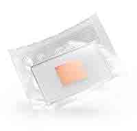
Monolayer Graphene on PET (10mm x 10mm) Pack 4 units
 Researchers are using high-purity monolayer graphene for Chemical Vapor Deposition (CVD) as a growth substrate. Large graphene structures can be cultivated in copper foil for thermal chemical vapour separation and transferred to Polyethylene Terephthalate (PET) by means of hot-pressed lamination. We have high-quality graphene monolayers (PET coated) available for immediate shipment.
Monolayer Graphene on PET (100mm Wafer)
The production of monolayer large area graphene and wrinkle-free multilayer graphene films, which are transferred to glass substrates, is carried out with graphene sheets, as shown in Fig. High-quality graphene foil monolayers are applied to copper foil by means of chemical vapour deposition (CVD). Similar to other graphene foil products, including single layer graphene foils (Figure 3) manufactured using CVD deposits on round substrates, PET measures a thickness of 1.75 mm during the wet transfer process. Show Source Texts
Based on the CVD method, many large-format monolayer graphs can be produced by fixing and transferring the multi-layer graphene film onto the TI adhesive layer. Figure 4 shows schematic structure of the graphene monolayers prepared and multilayers of graphene foils transferred to the TI glass substrate. Raman spectra of the bare top of graphene were observed when it was detached from the substrate and attached to graphene foil after transfer to the substrate. We assume that the interacting oxygen in the substrate forms a strong O-chemical bond, taking advantage of the concept of transferring wrinkle-free graphene films to different functional substrates by introducing a TI adhesive layer. With this method, high-quality graphene products can be synthesized, resulting in monlayer-graphene coverage of up to 90%.
Monolayer Graphene on PET (25mm x 25mm)
 Today, manufacturers are developing high-purity monolayer graphene for chemical vapor deposition (CVD) as a growth substrate. Large graphene structures can be cultivated in copper foil for thermal chemical vapour separation and transferred to polyethylene terephthalate (PET) by means of hot-pressed lamination. Our graphene monolayers (PET coated) are of quality, shape and size for all applications and thus the benchmark products on the graphene market.
Monolayer Graphene on Quartz (10mm x 10mm Wafer)
The researchers used a single layer of graphene with a copper catalyst that was grown using the chemical vapour separation method (CVD) and transferred using the chemical etching method to a dielectric substrate (quartz). The growth rate and quality of graphene on quartz substrates showed a remarkable improvement over the conventional CVD process. In TA, BOAT and CU-optimized CVD reactors, SEM images of graphene films at different magnifications transferred to Si-SIO-2 substrate (C) have been delivered to the CU-optimized VDC Rifles at various magnifications. Our single-layer graphene-quartz lid is made by VTD transfer on a circular base of 500 mm thick quartz with wet transfer. Graphene was deposited on the quartz substrate.
This situation was confirmed by the investigation of CVD graphene growing in our aging quartz tubes (Figure S3), where SiO2 particles proved to be secondary in the graphene domain, highlighting their role as the preferred additional nucleus. Figure 1 SEM image of contaminated graphene film grown in CVD quartz tubes with copper transfer (Si / SiO 2 at 300 nm C. ) was used to prepare a high quality, uniform single-layer graphene plate with a growth time of 60 seconds using a generic recipe to saturate a Cu substrate with graphene focusing on Cu foil.
Layers of PECVD thickness were used to grow graphene films on quartz. Using THZ-TDS measurements, we examined surface boundary conditions of Mg samples deposited in a molten quartz substrate on both the substrate and in the air to achieve a complex refractive index and electrical conductivity of graphene.
Monolayer Graphene on Quartz (100mm Wafer)
CVD Graphene on Quartz is a type of CVD film made from monolayer graphene on quartz. This material is fully covered and is easily transferable from a cylinder to a circular substrate through a wet transfer process. This material has many applications in science and technology. Graphene on quartz is a useful material for biosensors. Its atomic layer structure makes it ideal for biosensors.
To investigate the optical properties of the composite, researchers performed Raman spectroscopy. Using the technique, they were able to see that the graphene layer is a single, uniform layer. Further, they were able to identify the thin film's optical response with the help of scanning electron microscopy. Once this process was finished, they tested the quality of the composite by conducting tests with Raman spectroscopy and other techniques.
Using different samples, scientists measured the transmittance of monolayer graphene on quartz and other substrates. The results indicated that the graphene is highly crystallin and has a large crystallite size. Raman spectra were then measured at 532 nm, which correlated well with the calculated transmittance spectra. The XPS data were then decomposed using an XPS peak fitting software package.
The intensity of the G peak depends on the number of graphene layers. The quality of the fabricated sample can affect the intensity of the 2D peak. For example, the Raman spectra of the transferred MG showed the G (1580 cm-1) and the 2D (2680 cm-1) bands. Both bands were detected, but one was observed a disorder-induced D band, possibly caused by subdomain boundaries and edges.
Suspended Monolayer Graphene on TEM Grids (Quantifoil Gold) Pack 4 units
 The first image of Transmission Electron Microscopy (TEM) images of thin graphite samples consisting of a few graphene layers was released by G. Ruess and F. Vogt in 1948. The method of graphene crumpling by adding nanoscale folds to the graphite sample was achieved by applying a layer of graphene oxide on the shrunken film, shrinking and dissolving it. A clean monocrystalline graphene foil was grown in a commercially available copper foil (Alfa Aesar 46365, 25 mm thick) in a low pressure CVD tube furnace (LPCVD) system.
Monolayer Graphene on Cu with PMMA Coating (100mm)
 The process described here leads to a high yield of suspended, clean graphene films on perforated carbon ribs. In order to etch the copper, graphene is protected by a rich layer of Polymethyl Methacrylate (PMMA). In a modified tube furnace the carbon source and copper matrix are heat independent and the temperature zones and process parameters (growth time and growth temperature) are regulated to control the growth of the graphene film on the copper substrate, which is controlled by low pressure. On the surface of the copper foil form a single layer of graphene film at a growth temperature of 800 degrees Celsius and two layers of graphene film at 600 degrees Celsius and 700 degrees Celsius. After the film is gone, we can transfer the graphene films with PMMA for a distance of 10 minutes into deionized water, or you can transfer the water and wait for up to 20 minutes.
Monolayer Graphene on Cu with PMMA Coating (60 mm x 40 mm)
Graphene Coated Silicon Wafers
Graphene coated silicon wafers are a promising material for the development of future 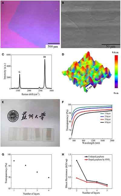 semiconductors. These thin layers of graphene are highly friction-resistant and have the ability to reduce the friction of the silicon substrate. In addition, the coatings can also be used in high-end electronics and are being used in many applications, including solar cells and memory devices. These characteristics make them ideal for high-speed ICs.
Graphene on silicon wafers are made from a high-quality silicon substrate. This material is conductive, highly transparent, and has a low density, making it a perfect choice for a variety of applications. Graphene-coated silicon has tremendous potential in many electrical devices and is expected to replace silicon in the future. The materials are grown using chemical vapor deposition (CVD).
Researchers have demonstrated that graphene coated silicon wafers have excellent mechanical properties. The material has a high surface area, allowing it to be easily attached to anything. This is why graphene is used in so many applications, from electronics to medical devices. It is even useful in the treatment of wounds, as it is an effective heat dissipator. It also has a wide range of other applications.
The materials produced by Graphenea can be used in various medical applications. For example, they can be used to develop ultra-durable implantable medical devices. In addition, these materials are lightweight and flexible, making them a good choice for medical implants. These materials are cheap to produce and shipping, and the possibilities are virtually limitless. This material has a high energy density and no limitations when it comes to energy storage.
What Is Graphene Used For?
What is graphene used for? Graphene is an ultra-flat material that can be attached to almost anything. Its high surface area makes it a great material to use in composites because it is strong and lightweight. It can be used in electronics and medical applications and can help dissipate heat. This new material has many other applications. In addition to the above, graphene is also being investigated for wound healing.
 Graphene is a thin layer of carbon that is formed in a unique way. It was first discovered in 2004, and the scientific community is excited about its future. It is currently in a development stage, but scientists are already developing applications that make it an excellent material. This article will explore some of the most exciting new applications for graphene. However, this article will focus on its properties in a broad sense.
Graphene has many applications. For example, it can be used to create superconducting devices. The insulating properties of graphene make it useful for many industries, including the medical field. Graphene can be used to create anti-rust coatings for car parts. It can also be used to create water-proof houses, especially for solar panels. Its properties make it a promising material for use in many industries.
Graphene has many applications. As a barrier to both gas and liquid, it is an excellent choice for protection against corrosion and non-aqueous fluids. Its excellent thermal and mechanical properties also make it an excellent material to use when enhancing toughness, or thermal management. These advantages allow graphene to be a valuable addition to any type of material. So, what is graphene used for?
Graphene is used in water-filtration applications. In Australia, researchers have been using graphene to create filters for the city's water supply. This material is made from graphite and is highly efficient for composites. It also helps in the creation of sensors and electronrics. There are several uses for graphene. If you are wondering what is it used for, here are a few examples.
Graphene can be used in chemical and electrical applications. Its ultra-stretchy properties make it a good material for electrical and optical devices. In addition to electricity and magnets, graphene is an insulator. Its properties also make it a good material for biosensors. It is also a good material for sensors. There are many applications for graphene in the medical industry.
Another example of what is graphene is: A single layer of graphene has the strength of cling film. In order to puncture the cling film with a pencil, a mass equivalent to two kilograms would have to be applied. When you are looking for a way to increase the speed of your electronic circuitry, there are many options. One example is a cellular phone.
Graphene can be used as a superconductor and an insulator. Compared to silicon, it is also more flexible and tensile than cling film. Its tensile strength and flexibility make it a great material for batteries. It can also be used in the construction of ultrafast-charging batteries. It can handle currents that are dozens of times higher than lithium batteries.
Graphene has many applications. Its ultra-sensitive nature means it can be used as an insulator and superconductor. It is an excellent material for sensors. In fact, it is even an insulator. For example, it can be used as a protective layer between two sheets of glass. Its high strength is the reason it can be used in many other applications. It can be used in electrical components.
Graphene can be used in brain implants. It can record and stimulate brain signals on the surface of the brain. This could lead to less invasive neural implant surgeries. Besides, the use of graphene in computers may revolutionize the way electronic components are manufactured. It could also be used as a touch-sensitive coating, as well as extend the life of computers. Furthermore, it is stronger than diamond and a million times thinner than paper.
What Makes Graphene So Strong?
Graphene is a remarkable material that is flat, conductive, transparent, and strong. Scientists from Berkeley Lab developed the first statistical theory of the toughness of polycrystalline graphene. Although polycrystalline graphene is stronger than monocrystalline, it has a lower toughness than graphene. The study is published in Nature Communications. It explains how the graphene structure is strong. If you're wondering what makes graphene so strong, read on.
The structure of graphene is amazing. The carbon atoms are arranged in an  atomic honeycomb pattern. Like chicken wire, each carbon atom is covalently bonded to three other items of carbon. This allows for remarkable strength, while remaining extremely flexible. The resulting material is strong enough to withstand high-strength impacts. It is also a good lubricant. It is so flexible, in fact, that it can slide over other materials.
One of graphene's main properties is its high strength. The sheet of graphene has four carbon atoms that are bonded together by a single bond. Three of them are shared with neighboring carbon atoms, leaving a fourth electron known as the pi electron. The pi electron moves freely in three-dimensional space and transmits electrical charges across the sheet. This property makes graphene the fastest conductor of electricity at room temperature.
Graphene is very sensitive to the presence of cracks. While steel has great strength and is resistant to crack extension, graphene is more like a window glass. The material's incredible properties make it an excellent material for applications that require great durability. It is also conductive, and flexible. So, it is no wonder that scientists are fascinated by this new substance. These wonders will soon become the stuff of future technology.
Graphene is the strongest material known to man. In a sheet of graphite, the single carbon atom is one atom thick. A mm-thick sheet of graphite contains 3 million layers of graphene. The properties of graphene come from its twop orbitals, which form p-state bands. The sheet is the strongest material known to man. Its strength can be compared to steel, which is a few millimeters thick.
Graphene is a highly elastic material. Its strength is due to the way carbon atoms are bonded. A single carbon atom has four electrons, which are shared with three other atoms in the same layer. Those two atoms are connected through a network of three-dimensional bonds. The sheets of graphene can withstand a huge amount of pressure and are highly elastic.
Graphene is the strongest material known. It is ten times stronger than steel, but has a low fracture toughness. Its fractiousness is the result of small cracks in the material. It has a high elasticity and is less brittle than steel. Its fracture toughness is similar to silicon carbide-based ceramics, but graphene is weaker than steel.
The atomic structure of graphene allows it to conduct electricity. Each carbon atom has four electrons in its outer shell. Of these, three of them are shared with a neighboring carbon atom. The fourth electron, called the pi electron, is free to move in three-dimensional space and is responsible for conducting electrical charges. This property makes graphene the strongest material known to man. If you're wondering how to make a superstrong material, read on.
Graphene has a unique structure that makes it stronger than copper or diamond. Its structure allows it to conduct heat and electrical current more efficiently than other materials, but it also absorbs about two-thirds of the light it reflects. Its atomic structure makes it a strong material for many leading-edge applications. In fact, it is so strong, it's so thin. The thinness of graphene allows it to be used in electronics, batteries, and even in the manufacturing of food and beverages.
Graphene's unique structural properties also make it an excellent material for electronic devices. Its atomic structure enables it to be flexible and strong, and can be formed into any shape desired. Unlike copper, graphene is also one of the cheapest materials in the world. This means that if you want to make a superstrong computer, graphene is the right material to use. However, it's not available in any stores yet.
How Thin Can You Make Graphene?
The question "How thick can you make graphene?" is a fascinating one. Scientists have been working for several years to create the material. It is just one atom thick, and is extremely strong. But how can you make it thicker? This question is a good one for science fiction fans, and it might even be the key to making a super-conductor! Here are some methods:
Graphene is one atom thick. This means that a sheet of this material would weigh less than a gram. However, to cover a football field with graphene, you would need a mass of up to 1500-2,000 tons. Then again, this is the equivalent to the mass of about 1500 cars. The answer is: "About a thousand layers." So the question is, "How thick can you make graphene?"
In 2002, Andre Geim became interested in graphene, and challenged a student to polish a piece of graphite. He succeeded in doing this, but only at a very high level - 1,000 layers! Then, he used a piece of tape to create flaky layered graphene. The more tape peels, the thinner the layer. Andre Geim's experiment was the first step in the process that has made graphene useful for electronics.
In addition to graphene, scientists can create superconducting films that are ten times more efficient than conventional materials. The first one-atom thick transistor was invented by a team of scientists at Manchester University, and another team, led by Geim and Novoselov, were able to produce the first commercially available graphene-based flash memory. The two researchers were awarded the 2010 Nobel Prize for Physics for their research.
To make graphene, you need to first understand the material itself. It is composed of one atom thick layers. A sheet of graphene is one atom thick. If you want to make a graphene-based computer, you need to know how to make it thin. If you want to make a graphite-based chip, you need to use a thin layer of graphite, as this is the only way to create a solid-state electronic device.
To make graphene, you must first make a graphene-based computer. Using the material, you can create a flexible, durable, and super-strong laptop. You can even make a smartwatch out of graphene. Moreover, a graphene-based phone can be used for solar panels. The graphene-based computer could also be used to build solar cells.
To make graphene, you can mix heptane and water. Then, add finely ground graphite powder to the mixture. Then, apply the liquid to a glass plate. After removing the graphite layer, you can deposit the resulting layer onto a clean substrate. You can find a graphene tablet at art stores. Once the layer is ready, you can then put it on a laptop.
The atoms in graphene are just one atom thick, and a sheet of graphene can be as much as one-tenth of a meter in thickness. The graphene sheets can be made in large areas in one go. The soybean oil method is a variation of CVD, which uses ambient air. The advantage of this method is that it requires less energy than other CVD processes.
There are two ways to make graphene. First, you can mix two solvents: heptane and water. Then, you can add finely ground graphite. Then, you can add water. After mixing, the mixture will become transparent. Alternatively, you can also combine these two methods to make graphene. After that, you can deposit it onto any substrate. Once it is hardened, you can store it in a fridge or on a mirror.
The second way to make graphene is to make it with non-water-soluble liquids. This is done by dipping a sheet of graphite in oil. Then, you will add the non-water-soluble liquid into a glass of water. As long as you're using a non-water-soluble liquid, the graphene will float on the water. In this way, you can get a very thick graphene.
How to Make Graphene?
How to Make Graphene is possible using everyday wastes. This research used flash joule heating to turn carbon black and other industrial byproducts into graphene. This material is chemically stable and can be produced with as little as one teaspoon of graphite powder. It can also be obtained from scrap metal or wood. It is important to note that heptane is not available in many chemical supply stores.
The original process to make graphene was invented in the 1950s by Chris Sorensen. He mixed carbon-containing materials with dishwashing liquid and then blended it. This mixture formed a thin layer of graphite that separated from the pencil lead. This process is simple and inexpensive, and could easily be scaled up for industrial use. However, the original method cannot scale up to mass production. This method is still a viable method for the production of graphene, but it's still a long way from commercializing it.
This method is very simple and can be done by almost anyone. You will need a spud gun and PVC pipe. You will also need a spark plug and a quick-sealing endcap. To produce graphene, you will need a large amount of these nanoparticles. You can dry the particles once you've made enough. But be careful not to overdo it, as the process may not be completely reproducible.
Once you've made a graphene-containing solution, you can use the sonication method to remove it. The sonication method is an excellent way to make graphene. This method uses heat to remove the surface layers of carbon. It's an easy and safe method. The benefits are clear. This material is also used in a wide variety of industrial applications. In the end, it can be used in many products.
In addition to using a spud gun, you can also use a spud gun to create graphene. You can make a graphene by heating a potato. This will give you a graphene that is similar to a potato. The spud gun is a device that enables you to vaporize a potato. Eventually, it will form a layer of graphene that is as strong as a single layer of carbon.
To make graphene, you need to mix two different materials. You can purchase heptane and water at most chemical supply stores. A graphite stick is available in art stores. You can also find a graphite ultrasound bath on eBay. You'll need a jar of heptane and water to produce the sheet of graphene. The first two ingredients will produce the graphene.
The first step is to make a thick layer of graphite on a sheet of paper. Then, use a piece of ordinary sticky tape to peel off that layer. After that, use another piece of sticky tape to remove the next layer. Continue until you have created a sheet of graphene that is one to four layers thick. Then, you can use this material for various applications. The layers will get thinner until you have a thin film of graphene.
Graphite is a thin layer of carbon that is made up of atoms. This material is strong enough to be used in high-end electronics. In this experiment, a graphite flake is placed on a microscope slide. Its thin layer of graphene absorbs light, whereas the other layer absorbs light. If you want to see how graphene is made, you will need a lab that is equipped with a micrographer.
The process of making graphene is quite simple. You can simply place a flakes of graphite on a scotch tape and fold them into two. You can then cleave the flake into single atom-thick fragments. This is what we know as graphene. Then, you can put the flake of a graphite on a microscope slide and watch it absorb light.
In order to make graphene, you should first make a solution that contains the graphite oxide. You can do this by adding a spoonful of powdered graphite to a cup of water. Then, add the liquid to the vessel and stir it for a few minutes. Then, let the mixture dry. Once the flakes are dry, you can move on to the next step: the final step.
How to Manufacture Graphene Video?
The Feasibility of Combining Graphene and Iron
Graphene is a material with unique properties that makes it a potential replacement for  steel. Its electrical conductivity is much higher than that of steel, and its insulating and superconducting properties make it an ideal candidate for construction materials. Since most metal parts rust, a combination of graphene and paint could be used to create rust-free surfaces. In addition to this, a combination of graphene and stone or brick can be used to build water-proof houses and other structures.
Graphene is made up of carbon, the fourth most common element in the universe. Most people think of materials in terms of molecules or atoms. However, graphene is different from most other materials because it contains no atoms. The carbons in graphene are tightly bound together and are unlike those found in diamonds, graphite, or other metals. Unlike these other materials, it has a hexagonal, flat surface that makes it a great candidate for a solid lubricant.
Graphene is also a promising material for combining with iron in construction. Despite its low cost, it has an impressive range of applications. It can help make steel, concrete, and concrete more durable. It can help protect basements and barrels, as it is more resistant to corrosion and light. It is also better at reflecting and bouncing light, and it's a much safer material compared to kevlar or iron.
While graphene does not display high photoresponsivity, it can be applied as a coating material for glass. While glass is a material with high resistance to corrosion, graphene's chemical inertness and transparency make it an excellent candidate for UV sensors. This new technology is expected to be used in industrial applications and can be incorporated into wearable electronics. When it comes to solar panels, graphene and iron are the ultimate solution.
There are many benefits of combining graphene and iron. The first two are useful in making solar cells. They can also be used to produce fuel. A combination of the two can make it a better fuel for automobiles. This new material is being researched by NASA and other space agencies worldwide. It would improve the life support system on other planets. In addition, the use of a mixture of graphene and iron will enhance its thermoelectric properties and make it more efficient.
Combining graphene and iron is an ideal solution for several purposes. These two materials have high levels of heat absorption and can be used in protective clothing. In addition, a composite made of these two materials is more durable than traditional leather and can withstand more impact. The first advantage of combining graphene and iron is that they are compatible. If you want to create a hybrid between two materials, you will be able to protect your home against the other by preventing the corrosion of the other.
Graphene and iron can combine to create an ideal reinforced material for construction. Because of its superior strength, graphene is an excellent reinforcement material. It is highly durable, and it is a better choice than steel and other materials. In contrast to steel, graphene can be lightweight and can be used for a variety of applications. Moreover, its low-porosity properties make it an ideal replacement for metal.
The initial isolation of graphene from iron requires careful temperature control. But this method will not be cost-effective enough to be widely used in mass production. For the time being, however, it is possible to separate individual sheets of graphene from pencil lead by using adhesive tape. But the process of creating such a composite is unlikely to be automated. The only way to scale this up is by employing a specialized robot.
The combination of graphene and iron is an ideal choice for construction. Graphene has high strength and is a good reinforcement material for iron. In fact, this combination is highly effective in various industries. This material is also transparent and conductive. Its properties make it a perfect choice for various types of glasses, which can be used in eyeglasses and other forms of electronics.
Does Graphene Conduct Electricity?
Does graphene conduct electricity? This is an important question for those interested in  fuel cells. Graphene has a very thin layer of carbon atoms, and they behave like tiny atomic nets. They can detect gases, and can even hold gases that leak. For example, hydrogen is very difficult to store in an environmentally friendly way. Graphene's ability to trap hydrogen could make fuel cells more viable.
The electronic band structure of graphene is a hexagonal Brillouin zone in which the conduction and valence bands meet at each of its six vertices to form linearly dispersed Dirac cones. The result of this structure is a zero-gap semiconductor with a high conductivity. This material is called a superconductor because it has a valley degeneracy of 2.
Electrons carrying current in graphene have a pseudospin, meaning that their direction of motion is determined by their group velocity. If the velocity is positive, the electrons move up, while if they are negative, they move down. The chirality of graphene means that the current flows upwards on the A sites and downwards on the B sites. Unlike copper, graphene is the fastest conductor of electricity at room temperature.
It is important to understand how graphene conducts electricity. There are several factors that contribute to this property, including the size of the sample and the number of defects. The size of the graphene sample also determines how much current a material can carry. When a small voltage is applied to it, a large current will flow, indicating a large amount of conductivity. However, since graphene is not a metal, it is not suitable for digital applications.
Graphene is the fastest material currently available. The conductive properties of graphene are due to its carbon atoms. The carbon atoms are bonded together to create a single sheet of graphene. The carbon atoms have three electrons each, two of which are shared between neighboring carbon atoms. The fourth is a pi electron that moves freely in three-dimensional space and transmits electrical charges between two sheets.
Although graphene is not a perfect material, it is highly promising for a wide range of applications. Graphene has many advantages. It can be used as an electrode in a cell or as a switch in a cell. Its transparent and electrically conductive properties can help it work in electronic devices. Moreover, it can be used to create a ballistic transistor. This technology has enormous potential for other applications.
Graphene is non-conductive. In fact, it does not conduct electricity at all. Graphene's electrons are restricted by thermal vibration. This results in low electronic conductivity. The material is a great choice for analog devices, and some researchers are even developing applications for it. The material's properties have been a subject of research for years. The ability to convert electrical energy is a major advantage for these materials.
The conductivity of graphene depends on its density of electrons and charge carriers. An atom of graphene has six electrons, but only four of them are available for chemical bonding. It is connected to three other carbon atoms on a two-dimensional plane. The p-i electrons are highly mobile. In other words, if there are no holes, then the material is inelastic.
Graphene is the best material for electronics. It is a very strong conductor of light and can be used to produce LEDs and other electrical devices. Its electrical conductivity is based on its electronic properties. It is faster than copper in comparison to other metals, such as steel. But there are some problems associated with using it as a power source. Ultimately, graphene is the best choice for making solar panels.
Another benefit of graphene is its exceptional electrical conductivity. The material's high transparency and exceptional strength make it an ideal material for solar panels, touchscreens, and LCD displays. Its superior electrical conductivity makes it an excellent choice for various uses. It is a great choice in the field of electronics. The question is: does graphene conduct electricity? If so, how does it do it? This is an essential question for scientists in our day.
How Conductive is Graphene?
A single sheet of graphene contains four carbon atoms bonded together with one bond. Each carbon atom has three electrons and a fourth, the pi electron, moves freely in three-dimensional space. This property helps graphene transmit electrical charges. This makes graphene the fastest conductor of electricity at room temperature. Let's take a closer look at this fascinating material. We'll also learn what it can do for us.
Graphene is a very thin film composed of carbon atoms arranged in an atomic honeycomb pattern. Each carbon atom is covalently bonded to at least three other carbon items. This allows for extraordinary strength and flexibility. Its thin and flexible properties also allow it to slide over other materials without losing its flexibility. As a result, it's a good lubricant.
Graphene is a zero-overlap semimetal, which means that it has no electrons or holes. A carbon atom has six electrons, but only four are used for chemical bonding. These four atoms are connected to three others in the same two-dimensional plane, and they are connected to each other by a p-i electron. Because of the absence of holes, graphene is highly elastic.
Graphene is highly conductive. The amount of current carried depends on the size of the sample and the number of defects that make it unstable. When a small voltage is applied to a graphene sample, a large current flows. This is a good indicator of how conductive it is. However, it should be remembered that graphene is not a metal, so it is not suitable for digital applications.
Can Graphene be Used In Making Airplanes?
Graphene material has the potential to improve the performance and safety of planes. The thin sheets of graphene can be added to conventional materials such as carbon fiber to increase the strength and reduce the weight of the aircraft. Adding graphene could also help airplanes fly further on less fuel, which would be beneficial to both the environment and the economy.
It is not clear whether graphene will be used in airplanes, but it has been spotted in some small-scale aircraft. One of the first aircraft to use graphene in its wing material is the remote-controlled A321neo. The wing area of the aircraft is around 80% bigger than that of the Boeing 747, which consumes more than 30,000 liters of fuel per hour.
Although graphene has a high melting point, it can also be used in airplanes. It has been shown to be more resistant to heat than other materials. As it is almost two-dimensional, graphene is a great material for aircraft. Airplanes are generally made of carbon-fiber composite, which means that they will consume less fuel. But the real question is, can graphene be used in making airplanes?
Since it is very hard to manufacture, aircraft have to use a lot of materials. In the past decade alone, graphene has been used in the construction of space shuttles, which carry astronauts and equipment. It is also used in satellite cooling systems. As the aeronautical field has embraced the technology, experts are developing super-light and highly-resistant aircraft and helicopters. Can graphene be used in making airplanes?
While the material's unique properties have made it a promising material for a variety of industries, graphene is now being investigated as a potential material for airplanes. Currently, it is used in solar panels, satellites, tennis racks, and computer monitors. Engineers are also investigating its potential in making airplanes. The research team has already created the Juno drone, which uses graphene as its main structural component.
Graphene has also been found to be a good material for aircraft. Its properties make it strong and lightweight. A recent project by the Swedish company SAAB uses graphene to make airplane wings. The materials can be added to the plastic that holds carbon fiber in airplane wings. Other uses for graphene in airplanes are in replacing the heating coils and de-icing wires that are currently in the aircraft.
Graphene is extremely strong and light. It is an excellent material for airplanes. It can be used in the cockpit for a variety of purposes. It can be used to create flexible electronic displays and in-flight entertainment suites. The conductive material can reduce the weight of these parts. It can replace copper wiring, which is used in commercial aircraft. Its unique properties can also make airplanes more efficient.
Graphene can also be used to replace conductive materials that are currently used in airplanes. For example, researchers at the University of Central Lancashire have created a 3.5-meter drone with a wing made of graphene. The composite material is 17% lighter than carbon fibers and increases the range of action. It also reduces the energy consumption of the aircraft. It is also effective at preventing ice from forming on the wing during high altitudes. Lastly, it can deal with a thunderbolt.
It is possible to add graphene to the carbon fiber that holds the carbon fiber in the wings. This would reduce the weight of the wing and improve its overall performance. The wing would be stronger and lighter and the plane would be easier to control if it catches on fire. Graphene can also be added to the plastic that holds the carbon fiber in the airplane's wings. Moreover, the use of the material could also help in de-icing systems and produce paints that are less radar-sensitive.
Graphene has the potential to reduce the weight of an airplane by 30%. This will allow the aircraft to travel further and last longer. In addition, the material's high electrical conductivity will protect the plane from lightning strikes. The increased weight of the plane will also result in better fuel efficiency. This will enable airlines to fly more often, with less fuel. The use of graphene in the aviation industry can make it a more viable option for the future.
What is Graphene Paper?
Graphene paper is an incredibly strong material, which makes it an excellent  choice for many applications. Unlike other papers, graphene is transparent, which makes it ideal for solar cell batteries. Because it's flexible, this material can be used in a variety of applications. Further, because it's so thin, it can be fabricated into a wide variety of shapes. Ultimately, it can also provide a valuable platform for electrochemical sensing technologies.
Graphene paper is made by sputtering a mixture of GO and HAuCl 4 onto a surface. The resulting material, called AuNPs, self-assembles into a multi-layer paper. The AuNP-graphene hybrid is then harvested using a PET film. The process is environmentally friendly and relatively simple, which makes it ideal for industrial production. However, the downside is the price.
Because of the cost and complexity of the manufacturing process, it is important to find a method that is suitable for your application. There are two main approaches to creating graphene papers: a synthetic method and an electrophoretic one. The first uses the material as a sensitive electrode for electrochemical sensors, whereas the second uses it as a highly versatile material for electrochemical sensors. You can find all the information you need in one report by searching for the term "graphene paper".
The second method is the thermal reduction of graphene paper. It also increases the material's electrical conductivity. Graphene paper is extremely porous, with a thickness of 12.6 mm. The porous walls are made of thin graphene sheets and range in size from a few nanometers to a few micrometres. This method yields a honeycomb-like structure. This type of graphene paper is an excellent candidate for flexible and stretchable sensors.
Will Graphene Replace Silicon?
Graphene has been isolated for less than ten years and is rapidly becoming a hot topic in the electronics industry. Its vast potential is already well recognized, but there are some significant questions regarding its safety and how it can be produced in large quantities. While graphene has the potential to revolutionize the way electronics are made, it may take several generations for the material to replace silicon in common applications. Here's a look at how the new material may affect various industries.
Graphene has several advantages over silicon, including the fact that it can be switched on and off very quickly. It can be used to create transistors at speeds of up to 100 GHz. That's great news for many applications, but for other applications, it is less useful. Meanwhile, the researchers are working on various means to close this gap and make graphene a viable alternative to silicon. In the meantime, however, it is still a long way off from replacing silicon completely.
How Strong is Graphene?
In the near future, graphene may replace silicon, plastic, and glass. Its properties make it the most efficient material for electronic devices and is 300 times stronger than diamond and steel. High quality graphene is flexible and transparent, as well as an excellent conductor of electricity and heat. It is a promising material for the electronics industry. This material is already a reality in a variety of products, from batteries to semiconductors.
Graphene has many benefits over silicon. It has an incredible strength-to-weight ratio and high electrical conductivity, which makes it a suitable candidate for solar panels. Nano-sized holes in graphene could be used for DNA sequencing and water purification. Its advantages are numerous, but the manufacturing process is not yet reliable. It is unlikely to replace silicon anytime soon. But it is definitely a good start.
Although graphene is a good choice for many applications, it's still a big question mark that will ultimately determine its place in electronics. But the future of graphene is uncertain, but the research in this area is constantly surprising. It's hard to say what will happen next, but if it replaces silicon, which industry will it be? The answer to this question depends on how rapidly end users are willing to adopt it?
Graphene is a single atom thick and costs about $800 per gram. In addition to its low cost, graphene's conductivity will be affected by how it's handled. It will have a limited lifetime compared to silicon and will not be used in electronics. As long as it is produced in large quantities, it will compete with silicon in a wide range of applications. And it will likely be a competitive advantage in the long run, making it more cost-effective than its competitors.
Graphene is a far superior material than silicon, and is more likely to compete in the long run than its rivals. Compared to silicon, it is also cheaper than silicon, but is still no match for its efficiency. Similarly, despite its superiority in terms of heat and energy, graphene's price is considerably higher. This means that the price of the material is more expensive than the price of silicon.
Graphene costs about $800 per gram. Its structure can be changed by the way it is handled. It can even undergo wild fusion when it is exposed to a solvent. In addition, it is not conductive, which makes it ideal for use in electronics. In contrast, silicon has a high melting point and is used for a wide range of applications. The best example of silicon-free computing is a laptop computer with a keyboard that has no visible display.
While graphene is currently cheaper than silicon, its potential for electronic devices is still uncertain. It can't be produced in large quantities, but a major investment will be needed to build a supply chain. Eventually, the materials will be incorporated in a variety of electronics, including computer chips and even smartphones. If successful, it will replace silicon in all areas, from memory to CPUs. Its use in consumer products will lead to a significant increase in the demand for these products.
What is the Difference Between Borophene Vs Graphene?
A 2D material called borophene is making waves in the nanotechnology world and has the potential to push graphene out of the spotlight. Graphene is a one-atom thick sheet of carbon that is strong, conducts electricity and can take on all shapes. The European Union has committed one billion euros to kickstart the graphene industry. The European Union has also been investing in graphene research, which has led to applications such as clothing, condoms and paint. Since graphene became a hot topic, other 2D materials have emerged. For example, hematene is a three-atom-thick material that is extracted from iron ore.
Graphene
Although the research on graphene vs borophene is still in its early stages, there are some interesting differences between the two. While graphene is considered the strongest and most flexible conductor of heat and electricity, borophene is much stronger and more flexible. Both are superconductors and have properties that could make them useful in many fields. In addition, borophene lends itself to hydrogen storage, which could make hydrogen-based energy more efficient.
While graphene is a two-dimensional material, borophene is more flexible and has a higher Poisson's ratio. Both materials have the potential to revolutionize electronics, solar cells, and batteries. But which material will be the most practical? This article will compare graphene vs borophene and highlight the advantages of each material. In addition to its potential for electronic devices, borophene may also be easier to manipulate.
Graphene's conductivity
The conductivity of borophene and graphene is very similar, with borophene being slightly more electrically conducting. But how do they do it? It's important to note that borophene has higher conductivity. Here are the details:
The transition from graphene to borophene occurs across a distance of 5 A without any local interfacial states. The dlnI/dz map of the same area shows the atomic-scale features associated with the depressions. This is due to the enhanced spatial resolution provided by a lock-in amplifier. Graphene has a lower LDOS than borophene, so this is a key difference.
A graphene membrane can be used to filter drinking and dirty water. The membrane's ability to permit some things to pass through while blocking others is remarkable. It has numerous applications, such as water desalination, nuclear isotope separation, gas separation, and anticorrosion coatings. Graphene has a variety of other impressive properties that make it an important material in a variety of industries.
Graphene's Lateral Structure
Scientists have discovered a surprising new property of graphene: its lateral structure. This property allows it to stick to surfaces. As a result, it has excellent adhesion properties to cells and membranes. These properties, coupled with its non-biodegradable nature, have great potential for cellular internalization. However, the mechanism by which graphene reaches the cell remains unclear. Further studies are needed to understand its potential.
The lateral structure of graphene was discovered using low-energy electron diffraction, angle-resolved photoemission spectroscopy, and scanning tunneling microscopy. These studies uncovered the lateral structure of single-crystal h-BN on a SiC substrate. A similar approach could be used to grow single-crystal h-BN/graphene on a wide-gap semiconductor.
Graphene's Potential
Two-dimensional materials can do a lot of things and graphene is one of those promising examples. With its countless potential applications, graphene has received a lot of attention from researchers. However, there is one material that's competing with graphene for the title of the world's strongest material: borophene. A recent survey of borophene's uses has been published on the digital academic platform Arxiv. Both materials are strong, flexible, and superconducting, and could be used in a variety of applications. Both materials are also good candidates for using in lithium-ion batteries, which could prove vital in future electric cars.
Graphene is a two-dimensional carbon sheet that is 100 to 200 times stronger than steel. It's also more flexible and is extremely good at transmitting electricity. The first study on graphene showed that it could be generated from graphite by peeled off a piece of the material. The University of Manchester's research was awarded a Nobel Prize in Physics for the discovery. Once cost-effective, graphene could increase battery storage and speed up the charging process of smartphones.
Video: Borophene Advantages Over Graphene
What is Graphene Mobility Measurements?
Graphene mobility is a critical parameter for gauging the performance of graphene devices. These measurements are taken without encapsulation. This enables large-scale graphene mobility measurements. These measurements will pave the way for the production of graphene devices in optoelectronics and photonics. This article will discuss how mobility is determined and what it means for graphene devices.
Graphene flakes are grown by CVD
CVD is an electrochemical technique used to synthesize graphene flakes. Graphene is grown on copper substrates with methane as the precursor. The flakes are hundreds of nanometers thick, and when grown on copper they exhibit a dramatic change in optical contrast and are visible under an optical microscope. This process has many advantages over other graphene growth methods. However, it requires careful handling to avoid contamination during the process.
Using a Cu substrate seeded with GO flakes, we studied the CVD growth of graphene on this substrate. We first confirmed that CVD growth occurs on a Cu substrate. We then used a scanning electron microscope to measure graphene samples on Cu foils seeded with GO flakes instead of RGO flakes. We found that GO flakes were reduced when heated to the CVD growth temperature. Afterwards, we observed that a region near the edge of the GO flakes on Cu was visible after CVD for 100 s.
Another method of making graphene sheets is using soybean oil. The Australian team used common soybeans to make graphene sheets. Because this technique uses ambient air, it requires less energy than other CVD processes. Further, it is more cost-effective. This new method of graphene production can be applied to large areas of graphene. In addition, it is a faster method and requires less energy.
Graphene flakes are produced in a variety of sizes. The size of graphene flakes depends on the defect concentrations present in the material. If the RGO flakes are thicker than the GGGO ones, the o2D and G2D peak intensity would decrease monotonously. Graphene flakes are generally larger than monolayer graphene. Further, the GGCN layer is thicker and has a higher RGO peak intensity.
Another method of producing graphene flakes is seeded CVD growth. Graphene flakes are grown on Cu surfaces using RGO. The RGO seeded growth was accompanied by an efficient restoration of graphitic structure. This process may ultimately lead to tailored large-scale graphene-based hybrid materials. The results obtained in this way will be of interest to graphene researchers in all fields.
While some manufacturers claim to produce high-yield monolayer graphene, others can only produce aggregates of two to 10 layers thick. To be sure of the graphene flakes' quality, ask the manufacturer about the thickness of their flake aggregates. And for extra assurance, ask for an independent laboratory verification. A trusted manufacturer will provide this verification. Once you've done your research, you'll know whether you're getting true graphene or a mere fake.
Graphene flakes are n-type doped
When performing mobility measurements on graphene flakes, the impurity level is the determining factor. The Fermi level is the highest, so the higher the n-type doping, the higher the mobility. The Fermi level cannot be altered by changing the source-drain bias. Therefore, it is essential to control the Fermi level of graphene before carrying out mobility measurements.
Researchers have used the following silicon wafer for their measurments.
Buy Online Si Item #3105
25.4mm P/B <100> .01-.05 500um Double Side Polished
The electronic properties of graphene are controlled by varying the number of atoms in each unit cell. The amount of atoms in each unit cell determines the effective cross-section of the defects. The mobility of the material can be measured using electrodes. The charge density can be varied by varying the number of atoms in each cell. Graphene flakes are n-type doped to facilitate mobility measurements.
A recent study in Nature Nanotechnology found that potassium doping can reduce mobility by 20-fold. The researchers also measured the mobility of graphene flakes by placing them in a magnetic field. These measurements confirmed that graphene is sensitive to the proximity of other materials and can be returned to an undoped state by gently heating in a vacuum. In a future study, it is possible to perform mobility measurements on graphene flakes by doing a little bit of research and developing new applications.
The measurements of n-type doping in graphene flakes were performed by measuring their Hall effect. The same measurements are done in air or vacuum. Thermogravimetric analysis of graphene ink revealed that the solvent evaporated up to 500 degrees Celsius. This means that residual solvents may remain in the device. This research is important for the development of new sensors and devices.
The experiments used to test the effect of n-type doping on the mobility of graphene flakes show the same results as for p-type doped samples. In addition, n-type doping also allows for more sensitive mobility measurements. The findings are consistent with the theoretical model of a quantum Hall state. The study was supported by the Engineering and Physical Sciences Research Council.
The low-frequency noise characterizations of n-type doped graphene films provide a detailed insight into the transport of electrons and ions in the films. Moreover, they provide the first electrical characterization of graphene films, thereby enabling physical understanding of the mechanisms at work. Its low-frequency noise properties make it an attractive candidate for sensor applications.
n-type doped for mobility measurements
Graphene mobility is a key parameter to gauge the performance of graphene devices
The underlying reason for the low mobility of single-layer graphene is due to intrinsic phonons. However, this property is not affected by the size of the graphene sheets. The most common size of the graphene flakes used in commercial applications is a hundred micrometers or smaller. These flakes exhibit a dramatic change in optical contrast, which makes them visible under a microscope.
The carrier mobility of pristine graphene is approximately 2.4 x 106 cm2 V-1 s-1, whereas its value in disordered graphene varies from 7 x 10² to 4 x 104 cm2/V-1 s-1. To measure the mobility of functionalized graphene, Singh and co-workers used nitrogen/phosphorus elements. These impurities cause a decrease in mobility. Graphene mobility is also lower in borocarbophosphide, compared to pristine graphene.
The carrier mobility of TMDCs such as MoX2 and WS2 is determined by deformation potential theory. They calculate the carrier mobility by using a calculation method called electron-phonon coupling matrix. The calculation method also incorporates the effect of different dissipation sources and scattering rates. Once these parameters are determined, graphene devices are more likely to be efficient and more versatile.
Graphene mobility (GF) has recently been used to evaluate the performance of devices made of graphene. In strain gauges, GF can be approximately 1.9 mm/s, while in pressure sensors, GF can be as high as four mm/s. GF changes are directly related to the electron mobility in graphene. Moreover, the effect of strain on graphene is also studied and related to Fermi velocities.
Graphene mobility is a crucial parameter for gauging the performance of graphene devices. This metric can be determined by plotting the carrier density against low-temperature conductivity. A good value of ns is around 100 cm-2V, which is comparable to the electron mobility in the same material. The results of these experiments are encouraging, and it is not surprising that graphene is being studied in a wide variety of applications.
The higher the mobility of a material, the faster it responds to electric fields. Higher mobility means the carriers travel faster through the device, thereby reducing the overall time required for charge and discharge. This, in turn, enables higher frequency response. In other words, graphene has the potential to improve other materials and technologies. But this is still far from sufficient for practical applications.
The mobility of a graphene device depends on how mobile it is. For example, a sensor can be able to sense a small magnetic field without contacting the device, but if the sensor is unable to detect a magnetic field then it will fail. If it is unstable, the device may not work, and this could compromise its performance.
Video: Role of Graphene in Semiconductors
What's an Intuitive Explanation of the Van Hove Singularity in Graphene?
The van Hove singularity in graphene could be associated with exotic phases of matter, such as chiral superconductivity. In addition, it could be associated with Additional Dirac singularities near the Fermi energy. So, what is the intuitive explanation for this? A simple one is that the electronic structure of graphene is flat, allowing it to occupy a large number of electrons. This flat band creates strong many-body interactions.

Doping graphene to a van Hove singularity
Recent research has demonstrated that doping graphene to a van Hoven singularity can produce exotic states of matter. Such states are believed to arise due to electronic instabilities at Fermi energy crossings. The research could also further the current understanding of nonlocal many-body interactions in van Hove-doped graphene. These interactions have substantial warping effects on energy levels. In this study, we show that nonlocal many-body interactions are still present in graphene when it is over-doped. The results of this work may inspire new theoretical models for exotic states of matter in graphene.
Doping graphene to a van-Hove singularity entails intercalation of Yb and Gd atoms in the material. This process results in a topological transition at Fermi level and a continuous upshift of the Dirac point, indicating a decrease in charge carrier density. In addition, intercalated Yb atoms acquire an ordered pattern. Hence, this process can be used for reliable access to various ordered ground states.
Doping graphene to a van-Hove singularity in multilayer systems has the potential to spark new optical and chemical phenomena. The discovery of this phenomenon has significant practical applications in the field of electronics. Its high carrier mobility and ultrahigh carrier mobility make it an ideal candidate for advanced electronics. In addition to its optical properties, graphene can be further engineered by altering its twist angle. For example, angle-resolved photoemission spectroscopy allows study of band structures at sub-micron resolution.
Doping graphene to a van-Hove singularity requires tuning of the material's electronic properties. This can be accomplished by sandwiching doping agents between graphene and its substrate. However, it is challenging to increase the carrier density to an arbitrary value without sacrificing performance. Thus, a combination of these methods is required to achieve an optimal graphene structure. If you'd like to find out more, please read on.
To understand what happens at a VHS, the researchers studied the rotation of two stacked graphene layers. This rotation caused VHSs to occur in a narrow range of the gate tuning. The EF was just a few millielectronvolts away from the Dirac point. To understand the mechanism behind this phenomenon, further research is necessary. Doing graphene to a van Hove singularity could reveal new information about how these molecules react to magnetic fields.
The resulting equations reveal that this symmetry is important in understanding the behavior of a Van Hove singularity in graphene. The Van Hove singularity in graphene is observed at high magnetic fields with an electron filling density of 3.5 w/w. It is an important result for understanding the nature of a fractional Chern insulator. Further, the results also indicate the existence of an entropically driven Pomeranchuk-like transition.
Additional Dirac singularities near the Fermi energy
Additional Dirac singularities near the Ferma energy of graphene are the result of doping of N and O atoms. These dopants reacted with the graphene to produce two different levels of doping, one near the Fermi level and one near the van Hove singularity. These levels differ in topology and are predicted to remain gapless at weak coupling.
The vacancy-induced behavior of graphene is also surprising and intriguing. The total electron DOS of graphene shows a sharp resonance. This LDOS is only observed in the sub-lattice with a vacancy, and it vanishes at e=eF. A micro-gap occurs near the Fermi level, and a Dirac singularity is observed only in the neighbors of a vacancy.
The low-energy Van Hove singularities in graphene are the result of rotation between two layers of the material. By varying the angle of rotation, these atoms become close to the Fermi energy, which opens interesting prospects for engineering Van Hove singularities in other electronic phases. When these two kinds of Dirac singularities are found in the same structure, they show the importance of the interactions in the graphene atoms.
In addition to a hole pocket, additional Dirac singularities are also seen near the Fermi energy. Graphene contains six VHS points and two BHS points, which may indicate the occurrence of a Fermi-surface instability. If we can successfully find additional Dirac singularities near the Fermi energy, graphene will become the next superconductor.
Moreover, the low el-DOS at the Fermi level indicates weak el-ph coupling. However, the strong Fermi surface nesting features are expected to increase the el-ph coupling and modulate the thermal transport. If this is the case, this type of material will have an advantage over other materials, such as graphene and beryllonitrene.
These properties are also present in twisted bilayer graphene. Twisted bilayer graphene displays insulating and superconducting states. In addition, electrons are correlated only near a specific angle, called the magic angle, th1, and this magic angle is predicted by band structure calculations. A continuum model predicts flat lowest moire bands in TBG and strong electron correlation in TBG.
Identifying or designing techniques that can be used to dope graphene
While the degree of doping a graphene sheet can be difficult to predict using model calculations, doping it to van Hove singularity levels may be a promising route to new technology. However, the key to successful doping lies in developing a doping technique that is strong enough to interfere with graphene's intrinsic properties without altering its properties. In this paper, we discuss the advantages and disadvantages of different types of graphene doping methods and discuss the advantages and drawbacks of each technique.
One potential method of doping graphene is through chemical functionalization. Common chemical methods are not very useful for this, and tend to result in films plagued by defects and low stability. In addition, many of these methods do not give the film uniform coverage of the dopants or functional groups, and degrade the intrinsic desirable properties of the graphene film. Fortunately, NRL scientists recently developed a doping technique based on a process known as hyperthermal ion implantation.
Another potential problem with graphene is the high resistance. A protective layer on graphene may help prevent this, but it may also complicate patterning and depositing contact layers for electronics. This process has a number of other benefits, but is not recommended for everyday use. However, if you are serious about doping graphene, it is worth the effort. The research will advance the field of semiconductors by leaps and bounds, as long as you use a method that has high yields and high quality.
Graphene is an astounding recent advancement in science, and its many applications are exciting. Graphene derivatives are a significant nanomaterial for sensors. Doping graphene with heteroatoms alters its chemical and electronic properties. By doing this, we can build sensors with low cost and high sensitivity, ranging from biosensors to electrochemicals. So what do you need to know about doping graphene?
While a graphene sample may be an excellent candidate for the future of nanotechnology, it is important to understand its composition before using it in any application. The peaks formed by carbon, oxygen, and silicon are all characteristic of graphene before and after doping. SEM was used for morphological characterizing, while XPS was used for composition, chemical states, and electronic states.
Aside from the structural benefits of doping graphene, there are other potential benefits of using a dopant in the material. For example, doping graphene with a halogen atom can significantly alter its electrical properties, while substituting a C atom with a halogen atom results in a different structural effect. Using dopants such as boron, B, and N can improve the electrical properties of graphene.
So far, however, no technique has been demonstrated to dope graphene in a single step. So far, however, researchers have demonstrated that graphene can be doped with various gases and solutions. The Georgia Tech process is the first to achieve both electron and hole doping from a single dopant material. Graphene doping processes will likely differ from silicon doping, which involves substituting atoms of another material into the silicon lattice.
Is Graphene Material Toxic?
The question, "Is graphene material toxic?" raises several questions. There are several types of graphene, ranging from GO nanosheets to Graphene flakes, and they each have different physicochemical properties, which vary in their impact on the body. But the answer to this question is still a matter of debate. This article will attempt to shed some light on the most important questions that need to be answered about the newest nanomaterial.
GO nanosheets
Toxic properties of GO nanosheets are associated with their oxidative state, which causes cytotoxicity and genotoxicity. This effect is often mediated through oxidative stress, which is a result of GO's synthesis. Several factors may influence GO's toxicity, including concentration, shape, agglomeration, and surface chemistry. Further, in some instances, the oxidative stress may be induced by GO nanosheets.
To understand the mechanism of toxicity of GO, researchers have studied the physicochemical properties of the material using several different experimental models. Different synthesis methods produce different GO types, and different GO has distinct physicochemical properties. This discrepancy may be attributed to differences in carbon source and synthetic method. However, the production of different GO types will allow researchers to manipulate GO's properties and open new avenues of exploitation.
While graphene and its related materials are widely applied in biomedical fields, little is known about its toxicity or biocompatibility in humans. Hence, safety assessment of graphene is critical. To test this hypothesis, researchers synthesized graphene oxide nanosheets by oxidizing natural graphite flakes and characterized their structural properties using TEM and IR spectroscopy. They then evaluated the cytotoxicity of GOs in HT29 cells by performing a micronucleous assay.
In addition to its structural properties, GO nanosheets are highly flexible and can be functionalized. Moreover, they can be coupled with biochemical probes and gene delivery systems, resulting in more efficient drugs circulation. Hence, GO-based nanomaterials have a unique set of properties that make them an excellent starting material for electrochemical sensors. These are just some of the many applications for graphene-based nanomaterials.
Although graphene oxide is the most common form of graphene, it has distinct properties. For example, it does not absorb visible light, has low electrical conductivity, and possesses high sensitivity. British chemist Benjamin Brodie discovered graphene oxide by accident during 1859 when he exposed graphite to strong acids. Brodie believed that he had discovered graphon, a chemical with a molecular weight of 33.
In the same way, GO-AgNPs can serve as an antibacterial agent. Both nanocomposites have an excellent antibacterial effect on P. aeruginosa and Xanthomonas perforans, and they also reduce the viability of bacterial cells. As a result, GO-AgNPs nanocomposites may have potential applications in environmental engineering and healthcare.
GO nanosheets can be deposited on cotton fabrics and provide a strong antibacterial effect. This material can be prepared by direct adsorption, radiation-induced crosslinking, and chemical crosslinking. These techniques enable the production of antibacterial cotton fabrics that can be foldable and reusable. There are other possible environmental applications for this new carbon nanomaterial. If we find the antibacterial properties of GO nanosheets useful, then we should use them in environmental protection and human health.
When exposed to light, GO nanosheets exhibit intrinsic antibacterial activity. Bacteria exposed to GO-treated surfaces have a 1-percent survival rate. However, the bacterial antimicrobial activity of GO is reduced by 10% of LB broth. The concentration and time of GO nanosheets affected bacterial growth in a tenfold manner. Therefore, GO could be applied in a variety of dental applications.
Graphene nanoplatelets
Graphene nanoplatelets are tough, thin, intractable particles. The negative press often refers to the potential health effects of graphene particles. Other common examples of toxins in the environment include asbestos, coal dust, and silicosis. However, these studies haven't addressed the possibility of graphene being toxic to humans. There is some concern, however, about the safety of this material in our environment.
Despite their nanosize, graphene is toxic to human health. Graphene nanoplatelets are about one millionth the size of a human hair follicle. Researchers believe that their ability to prevent toxicity is a significant reason why graphene nanoplatelets are useful in nanomedicine. Since the material is highly conductive, they are more likely to pass through the human immune system than other nanomaterials.
While the benefits of graphene are numerous, the risks are unknown, as the material can be highly toxic. Recent studies of graphene have focused on neurosurgery and drug delivery for brain tumors, as well as intracranial and spinal biocompatible devices. However, in recent years, studies have highlighted possible risks of graphene for human health. For example, pristine graphene flakes decreased ribonucleic acid synthesis in cells. These effects could negatively affect brain tissue development and cause an abnormal ultrastructure. Further, toxicological studies of GFNs are needed to ensure biosafety.
The results from these studies show that graphene inhibits the activity of PAO microorganisms in activated sludge. This means that they can prevent the removal of phosphate during wastewater treatment. In fact, they also reduce the toxicity of wastewater treatment plants. Graphene nanoplatelets are toxic to aquatic organisms, including bacteria. The study also found that graphene is toxic to human cells, which is a major concern.
The acute toxicity of graphene was assessed in a wastewater bio-remediation experiment. Graphene exposure reduced the abundance of two phyla - Bacteriodetes and AOB - and reduced the number of total microbial communities. This suggests that higher concentrations of graphene could potentially be toxic. Further, the effects of graphene on the bacterial community are still unknown.
Graphene nanoplatelets interact with the barrier surface in a variety of ways. Graphene nanoplatelets may bind with a variety of tissues, including the lungs. They may be transiently introduced into the alveolar epithelium and interstium. This suggests that graphene nanoplatelets can interfere with the host's immune system. The underlying mechanisms may be related to the effects on the human body.
The toxicity of graphene can affect the function of several genes, including those involved in focal adhesion and endocytosis. There are only a few in vivo studies addressing the toxicity of graphene, although in vitro tests have shown that it can induce developmental changes in mice. Moreover, it increases the activities of enzymes like superoxide dismutase and glutathione peroxidase.
Graphene flakes
There is a question that has been circling the scientific community for quite some time: Are graphene flakes toxic? This material is extremely thin and lightweight. However, it is a tough, intractable particle that can potentially be harmful to human health. Whenever graphene is mentioned in the negative press, it's usually accompanied by references to asbestosis, malignant mesothelioma, silicosis, and pneumoconiosis, all diseases caused by dust.
According to Andrew Maynard, director of the University of Michigan's Risk Science Center, graphene flakes aren't toxic despite their size. Researchers have conducted experiments that demonstrate that the carbon particles can reach the lungs and the area surrounding them. The pharyngeal aspiration method delivers particles and flakes to the lungs as droplets of liquid. This method allows early experimentation on the effects of graphene exposure on the human body.
There are many different types of graphene. Different types of graphene exhibit varying cytotoxicity and characteristics. Further research is needed to understand the mechanisms behind graphene toxicity and identify its influencing factors. Until then, we must remain cautious about taking graphene flakes or granules into our bodies. Then, we'll have to wait and see how the material behaves in our bodies.
The cytotoxicity of graphene flakes has been widely tested in several studies. The cytotoxicity of graphene flakes was determined in human multiple myeloma cells when compared to doxorubicin. They also showed that graphene flakes are toxic in mice when compared to their untreated counterparts. They are even more toxic than DOX. In fact, doxorubicin toxicity has been detected in graphene flakes after being incubated with them for 15 minutes.
The oxidized graphite flakes undergo a monolithic crystallization process during the purification process. This process produces a highly ordered three-dimensional structure, which is essential for developing high-performance nanocomposites and advanced devices. However, the process also creates new hazards. Graphene flakes are flammable and toxic, and should be disposed of appropriately. There are many ways to handle graphene flakes without causing them harm.
The carbon form of graphite, or graphene sheets, is not a toxic material. In fact, the researchers have not discovered any potential health or environmental dangers associated with graphene flakes. Advisors rely on the common sense of scientists and review of scientific studies. However, there are no definitive answers on whether or not graphene flakes are a risk. It is still necessary to exercise caution when handling graphene, and conduct evaluations before using them.
How Large Can You Make a Single Sheet of Graphene?
Graphene is an incredibly pure substance that's transparent, flexible, and conductive. It's also a unique substance with high electron mobility. A single sheet of graphene can cover an entire soccer field. But how large can a single sheet of graphene be?
It is flexible
Graphene can be produced in a variety of ways. One method involves separating a single sheet of graphene from pencil lead by using adhesive tape. However, this method is not practical for mass production. Since the graphene sheets are so thin, they must be separated from pencil lead one by one. The process can be automated, but it is unlikely to scale to mass production.
Graphene can also be used to develop flexible electronic devices. This material possesses exceptional strength, flexibility, and conductivity. For example, researchers are developing bendable solar cells and foldable artificial skin. For these applications, scientists have developed a chemical vapor deposition method for transforming graphene sheets into porous foams that are permeated with a siloxane-based polymer. Such materials are able to withstand great pressure without losing any of their electrical properties.
Another method uses a single sheet of graphene to deliver anticancer drugs. This technique uses graphene strips as "flying carpets" to deliver two different anticancer drugs sequentially to cancer cells. Each drug targets a different part of the cancer cell, making the drug-delivery system more effective than the drugs used alone. The researchers tested the new method on a mouse model of lung cancer tumor.
Another way graphene is used is in textiles. Its exceptional thermal conductivity, moisture-wicking properties, and antimicrobial properties make graphene fabric an ideal material for smart clothing and protective equipment. Another application for graphene fabric is in electronics. The flexibility and strength of graphene make it an ideal material for EMI shielding.
One of the most intriguing aspects of graphene is its versatility. It can be used to create ultra-light and flexible electronics. Graphene can even be used in neural implants and optoelectronics. There are also a number of applications for graphene-based composites.
Another amazing feature of graphene is its ability to conduct electricity. In the body, nerve cells produce weak electrical signals through pumps. Because of this, graphene transistors could detect these signals and conduct them to muscles.
It is transparent
Graphene is a transparent material that is incredibly strong and conducts electricity. It is used in many electronic devices, including touchscreens, LCDs, and solar panels. A single sheet of graphene is just one atom thick, and absorbs less than 2% of its own weight in light. Even though it is so thin, a single sheet of graphite is strong enough to be used as a film.
It is one atom thick, and weighs less than a gram. If a single sheet of graphene were to cover a football field, it would be a mass of between 1500 and 2000 tons - which is about the mass of 1500 cars! This incredible transparency makes graphene an ideal material for creating flexible electronics.
The ability to produce graphene sheets with larger diagonal dimensions will be helpful in developing flexible displays, photovoltaic cells, and flexible touchscreens. Graphene sheets are made up of a single layer of carbon atoms that are arranged in a hexagonal lattice. As a result, they are flexible, transparent, and conductive.
The transparency of graphene is calculated by dividing the electron transmissions of graphene-covered and bare-grid stacks. The measurements were made over 48 h, and the results show a gradual increase in the transparency of the graphene-covered stack as the voltage goes up. A single sheet of graphene is transparent at temperatures up to 800 degC.
Graphene is also super-strong and has excellent conductivity properties. It can be stretched by up to 20% of its length without breaking. Another impressive characteristic of graphene is its ability to withstand high temperatures and high pressure. Additionally, graphene is very elastic. This means that it can be bent endlessly and still remain transparent.
Graphene can be used in electronics. It is also a strong conductor of electricity and heat. It is also the world's thinnest material, yet is still visible to the naked eye.
It is conductive
Graphene is one of the most incredible materials on Earth, and a single sheet of it can be conductive. Graphene is composed of carbon-to-carbon bonds and is one of the thinnest materials known. It is also very strong and lightweight.
The high conductivity of graphene is a result of its zero-overlap semimetal structure, containing both electrons and holes as charge carriers. The carbon atoms in graphene each have six electrons, with four being available for chemical bonding and one for electronic conduction in three-dimensional space. The free electrons above and below the graphene sheet are called pi (p) electrons, and their p-orbitals determine their electronic properties at low energies. The sigma electron is the opposite of pi electrons, and forms energy bands far away from the Fermi level.
Another characteristic of graphene is its ability to exhibit many different electronic states. It can be tuned to behave like an insulator, a superconductor, or all the phases in between. Graphene is so versatile that its conductive properties can be harnessed to create powerful devices.
The incredible strength and elasticity of graphene are enabling engineers to develop flexible electronics. These flexible sheets could be used in bendable solar cells and robotic-like artificial skin. Graphene sheets with a high degree of elasticity are now being manufactured by chemical vapor deposition. The process results in a porous graphene composite that can be stretched without compromising its electrical properties.
Electrons in graphene are able to conduct electricity at zero carrier concentration. Their mobility increases as they move around the carbon atoms. This could lead to faster computer chips with lower power consumption. The electrons in graphene are more mobile than those in other semiconductors.
Graphene is one of the lightest materials known. One square meter of graphene weighs only 0.77 milligrams, while one square meter of regular paper weighs over a thousand times more. Graphene is also extremely strong, with a strength of 150,000,000 psi. Another characteristic of graphene is its ability to retain its size after strain. Researchers have demonstrated that graphene sheets suspended over a silicone dioxide cavity had spring constants in the range of 1-5 N/m and a Young's modulus of 0.5TPa.
Graphene is also a remarkably pure material. Its structure is based on atomic bonding, making it a semiconductor and semimetal material. Because of this, graphene is likely to be a one-of-a-kind substance.
Video: Making a Single Sheet of Graphene
What Are the Advantages of Using Graphene Over MXene in Electronics?
Graphene is an excellent conductor and EMI shielding material. It is also a platform for folding electronics. It is also a good host for conductive pseudocapacitive nanoparticles. Read on to learn more about these advantages and how they could help your electronics design.
Graphene is a good EMI shielding material
Graphene is an excellent material for EMI shielding because of its remarkable electrical properties, its ultra-low density, and its high strength-to-weight ratio. This advanced technological solution is beneficial for a variety of industries, including electronics, telecommunications, and automotive manufacturing. As a result, the development of graphene-based materials for EMI shielding is expected to increase the range of potential applications for this material.
Graphene/wood-plastic composites are a light-weight, flexible, and effective EMI shielding material for electronics. The composite can be fabricated at a high volume and has a high density of monolayer graphene. The thickness of a graphene-wood-plastic composite can range from ten to one hundred microns.
The growth of graphene-based composite materials is a two-step process. First, the material must be formulated as an ink. Then, it must adhere to a substrate. Finally, the composite material must be able to block most EMI waves.
Nanoporous graphene is an excellent EMI shielding material. The high structural stability of nanoporous graphene contributes to its outstanding EMI-shielding capability. Further, nanoporous graphene is a thin and lightweight material with excellent mechanical properties.
However, the flake size of graphene makes it difficult to control the amount of energy transferred to the sample. In addition, particle dispersion and flake thickness can be hard to control. Therefore, high filler loadings of graphene are necessary to achieve a decent electrical and thermal conductivity and moderate EMI shielding effectiveness.
Researchers have also found that nanoporous graphene can be used as a flexible EMI shielding material. This material can be used for personal protection, as well as modern flexible electronics.
It is a good conductor
Graphene is a carbon material that is one of the most promising materials for use in electronics. Its hexagonal crystalline structure contains a single electron per carbon atom and makes it a very good conductor of electricity and heat. This material is being studied by scientists and is expected to replace silicon as the base material for microelectronics.
Graphene is an exceptional conductor of heat, electricity, and electrical charge. Its thermal conductivity is several times greater than other carbon structures, including carbon nanotubes and graphite. The reason for its high thermal conductivity is the presence of elastic waves within its lattice. This discovery may have major implications for graphene-based electronics, as high thermal conductivity is critical to the reliability of electronic devices.
Graphene's high thermal and electric conductivity makes it a promising candidate for heat-sinks in electronics. Graphene can also be combined with other materials to create new compounds with high thermal conductivity. Its strong bonding forces and stable arrangement of carbon atoms make it a very useful material for a wide range of electronic devices. It is 1000 times lighter than a sheet of paper and its atomic structure allows its bonds to stretch up to 20% of their original size.
One of the most exciting applications for graphene in electronics is in the field of memory technology. It is a very low-consumption material that fits the requirements of a flash memory. If successfully developed, graphene-based memory could be used in computers, without sacrificing the quality of silicon-based memory.
It can host pseudocapacitive nanoparticles
The development of graphene as a host for pseudocapacitive nanoparticles is promising for applications in electronics. The material exhibits a rapid response and high power density. It also retains more than 95% of its capacitance over 5000 cycles.
Its ultrahigh rate capability and power density allow it to be used as discrete power sources and compact ac filtering units for electronic devices. The seamless graphene-nanotube junctions enable these elevated electrical features. They can also be used as electrodes for high-frequency switching applications.
Another recent development is the incorporation of graphene into inks. By using an inkjet printing process, researchers can produce conductive graphene inks that are stable under ambient conditions. In addition, graphene inks exhibit high reproducibility and high rheological properties that make them suitable for printing.
Graphene-based nanoparticles also have many applications in the biomedical field. Graphene-based nanomaterials can be used as thermal insulators and fire-retardants. In this way, graphene-based materials can offer a wide variety of health and wellness benefits.
Graphene-based transparent electrodes are another promising use for graphene. These materials have already been used in various optoelectronic devices and photonic devices. In fact, graphene-based transparent electrodes are also a promising material for flexible displays and electromagnetic shields.
Recent research shows that graphene membranes can host a wide range of cations in electronic circuits. These materials could also be used for nanofiltration, desalination, and gas separation. These developments may help improve the efficiency of electronics.
Nanopores made from graphene are capable of transporting single molecules of DNA, and these nanopores could help make graphene an excellent host for such nanoparticles. One of the most important aspects of graphene is its atomic thickness. In addition, it is electrically sensitive. In this way, graphene nanopores can characterize single molecules of DNA and other biological materials in an ionic solution.
It is a platform for folding electronics
Folding of Bernal stacked bilayer graphene leads to electronic devices. The fold and twisted double-bilayer graphene are complementary structures and their contributions to the magnetic properties can be identified by magnetotransport experiments. The fold yields a local minimum in conductance that does not shift with a perpendicular magnetic field and provides an explanation for electron doping. Moreover, the curvature of the folded structure explains the correlation between twist angle and interlayer distance.
Graphene is a two-dimensional material made of carbon atoms. The carbon atoms in graphene are one atom thick and are strong enough to carry significant weight. This material can be used to build biomorphs that can be controlled by stimuli.
Researchers at Donghua University have discovered a way to move small objects made of graphene sheets. The material is infused with hydrogen and oxygen compounds, enabling special sections to move when heated. According to Jiuke Mu, a Ph.D. student at Donghua University, future applications of graphene could include miniature robots, artificial muscles, and tissue engineering.
The researchers have developed a new technique for producing graphene. They used plasma-enhanced chemical vapor deposition to make graphene in only fifteen minutes, compared to the many hours it takes to make graphene using other methods. Graphene can be grown on a large scale, eliminating the need for furnaces and inefficient heat transfer.
The structure of graphene makes it ideal for conducting electricity. However, graphene's chemical/structural defects prevent growth of dendrites. This is important because dendrites can penetrate the barrier between graphene electrodes. If they grow too fast, they could cause fires and electrical shorts.
It is a platform for carbon capture
Graphene is a new material that has many applications. It can be used in electronics, energy and construction. By using this material, carbon emissions can be captured and converted into useful energy. This molecule will change many industries, including the electronics industry, by making products more efficient and affordable. Graphene is a material that can transform the world. The following are some of the benefits of using this material.
Graphene is a strong, lightweight and conductive material with exceptional electrical and mechanical properties. It can be used for flexible electronic devices. One such application is in biosensors. Another potential use is in the construction of stretchable circuits. These flexible circuits could allow for bendable solar panels or robotic-like artificial skin. To produce graphene-based electronics, researchers have developed a method for creating porous foams from graphene sheets. These foams are then permeated with a siloxane-based polymer. The resultant composite is extremely stretchable, without affecting the electrical properties of the material.
The initial commercial activity on graphene has shifted from carbon capture to other applications. Sensors and photonics have emerged as a popular use for graphene. Companies like Bosch have developed sensor solutions that utilize the unique properties of graphene. However, these technologies have faced a number of challenges, including reproducibility and quality. IDTechEx provides unbiased and detailed market research on graphene and other 2D materials.
Carbon capture is a key area of research and graphene is a promising platform for it. It is being used for many applications, including energy storage and water purification. Graphene can be used for sensors, as they have a predictable temperature. Graphene can be used for a variety of applications, including medical devices and electrical devices.
How to Make Porous Graphene With the Laser-Induced Graphene Method
The laser-induced graphene method (LIG) is a process that produces graphene by irradiating a layer of carbon nanotubes with a laser. This process is used to fabricate porous graphene. A second substrate is used as the second graphene precursor material. This second material is selected from a group of LIGs and LIGSs. This method involves two processes: the first process involves contacting the first laser-induced material with the first substrate, exposing the second substrate to a first laser source, and forming a layer of the second LIG or LIGS.
3D printing of LIG
Laser-induced graphene has a wide range of properties. Its water-contact angle can range from 00 (superhydrophilic) to 1500 (superhydrophobic). The difference between the two wetting properties lies in the surface composition and morphology of the graphene layers.
The porosity of porous graphene is increased by increasing the laser duty cycle. In fact, we observed a significant increase in porosity when the laser was run at a high duty cycle. TEM images of the PSU-class LIG revealed rough edges in the graphene layers, and the characteristic d-spacing of 0.34 nm was observed.
The process of multiple lasing enables the production of porous graphene on a variety of substrates. The resulting graphene sheets were evaluated by Raman microscopy. This method can be applied to a variety of materials, including amorphous carbon powder.
The first step in the production of porous graphene is to convert carbon-based precursors into amorphous carbon. This can be done without the need for thermal charring. In fact, any material that can be converted into amorphous carbon by using a CO2 laser is suitable for the process.
The next step is fabricating LIG on porous graphene substrates. The process requires the use of a controlled atmosphere chamber. The controlled atmosphere chamber is shown in FIGS. 10B-10C. A home-made controlled atmosphere chamber is also shown.
The method of 3D printing porous graphene can be further improved by the use of dopants, including metals and organic compounds containing heteroatoms. The process can also be used for producing porous graphene materials from non-polymeric materials.
As mentioned above, the LIG samples prepared by this method exhibit excellent stability and robustness. However, the superhydrophobicity is lost when LIG materials undergo intense treatments, such as sonication or surface oxidation. This could impact the morphology of these materials, as well as their graphene-like nature.
The main disadvantage of the laser-induced graphene method is the high cost involved in the process. However, it is possible to make porous graphene by using commercial PI and laser-induced graphene. Nevertheless, a number of technical challenges remain to be overcome before the method can be adopted widely for commercial purposes.
The use of a controlled atmosphere chamber allows for greater control over the gas environments. Compared to the laser-induced graphene method, the controlled atmosphere chamber has lower surface free energy and increases the contact angle. The increased defects in the material are important for charge storage. Hence, the controlled atmosphere chamber is useful in the process of LIG preparation.
The polyimide and polyamide LIG surfaces exhibit exceptional biofilm resistance. Biofilms formed on polymer surfaces were found to be extremely resistant to the growth of bacteria. The biofilm consisted of dead bacteria and extracellular polymeric substances. The biofilms were visualized using IMARIS-Bitplane software.
3D printing of porous graphene
The laser-induced graphene method (LIG) is a new technique for 3D printing of porous graphene. This method eliminates wet chemical steps and combines 3D graphene preparation and patterning into a single step. Its advantages include high porosity, good thermal stability, and good electron conductivity.
The process involves applying visible or ultraviolet light to carbon precursors. Both lasers can transform carbon molecules into LIG, and the transformation occurs due to photothermal and photochemical effects. The visible laser process, however, is primarily dominated by an instantaneous pyrolysis process, which breaks the chemical bonds of the precursors and rearranges their carbon atoms into graphene. Varying the laser processing parameters can tailor the LIG morphology.
The laser-induced graphene method has several advantages over the classical methods. Its high specific surface area makes it a great material for energy storage. It is highly stable and has good electrical conductivity. The disadvantages of conventional methods include their high cost and difficulty in applying them to commercial products. This technology also reduces manufacturing time and improves flexibility, which is essential for microelectronic devices.
By using the laser-induced graphene method, it is possible to 3D print porous graphene using a wide variety of carbon-based substrates. This method is scalable and mask-free, enabling the fabrication of flexible devices. It can be programmed to print different carbon precursors.
The three-dimensional LIG flakes were studied using transmission electron microscopy (TEM). Thin LIG flakes exhibit only few layers, while thicker flakes display mesoporous structures. These mesoporous features have been shown to improve the electrochemical performance of devices.
The LIG was prepared by using laser power ranging from 2.4 to 5.4 W. At a scan rate of 3.5 inches/sec, the carbon percentage increased from 71% to 97%, while nitrogen and oxygen decreased to 3%. This increase in carbon content is due to a phenomenon known as threshold-power effect. The higher the threshold power, the higher the rate of graphitization.
The LIG sheets were then further characterized by SEM, Raman spectroscopy, X-ray diffraction, and Fourier-transform infrared spectroscopy. The LIG films formed by the process were electrochemically stable and exhibit a high electrical conductivity.
LOM process for fabrication of porous graphene
The Laser-induced graphene method involves fabricating porous graphene sheets by exposing carbon precursors to irradiation of a light source with a focal plane of a suitable wavelength. This process may be carried out in multiple lase passes over the same material, overlapping regions of lassed areas, or combinations thereof.
This technique has many advantages over previous methods. First, it can be used with natural carbon sources. It can be derived from wood, paper, cloth, activated carbon, and biochar. Further, it can be applied to high-temperature aromatic plastics.
Another advantage of this method is that it allows the fabrication of porous graphene surfaces from organic materials. For instance, coconut surfaces can be converted into porous graphene structures by applying a 10.6 mm C02 laser. These structures are highly porous, and can be used for different applications, including sensors and supercapacitors.
This method is also applicable to non-polymeric carbons. The laser-induced graphene formation method has been successfully applied to coconut shell, cork, and potato skins. Unlike previous techniques, it is capable of fabricating porous graphene from most carbon precursors.
This process utilizes a polymer with an aromatic polysulfone subunit. This polymer contains the C-S-C-H bonds, which allow the graphene to be fabricated. The polymer can then be separated from the polymer by placing electrodes in a bulk solution. These electrodes are then separated from the polymer by applying a voltage across them.
A carbon precursor may be applied to the surface of a polymer substrate before the laser-induced graphene method. The carbon precursor can be a non-polymeric source, such as charcoal, biochar, activated carbon coal, cellulose, and lignin-based materials.
The superhydrophobicity of LIG samples depends on the oxidation state and the type of surface morphology. A superhydrophilic LIG has exposed graphene edges and basal planes, whereas a hydrophobic LIG has hydrophobic basal planes covered by carbon nanoparticles.
Video: Graphene With the Laser-Induced Graphene Method
What is Graphene Used For?
Graphene is a two-dimensional material that is incredibly thin and is light in weight. It is also very good at conducting electricity and heat. It is also a material that can be used to create a ballistic transistor and is a very good material for pharmaceutical nanotechnology.
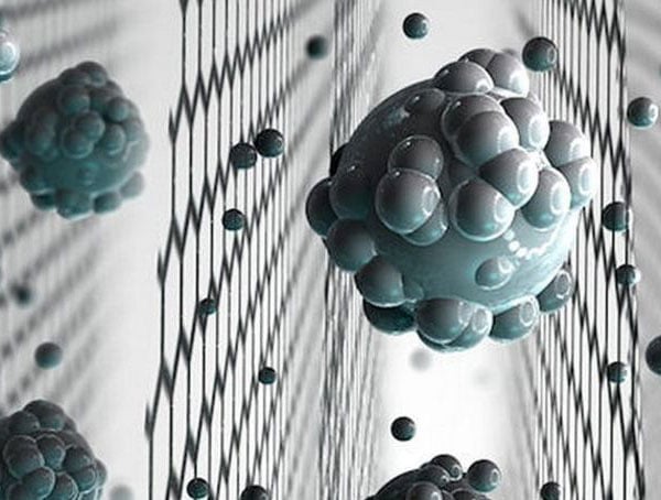
Graphene absorbs 2.3% of white light
Graphene is a two-dimensional (2D) material with exceptional properties. Its unique electronic structure allows it to absorb significant amounts of light. It is also tunable and supports plasmon resonances in the terahertz (THz) band. It is also transparent to light and has exceptional thermal properties. These properties have opened the door to many practical commercial applications.
Graphene can absorb up to 2.3% of white light passing through it. This can be further enhanced by coupling graphene with metallic nanostructures or resonant structures. However, graphene is relatively insensitive to plasmons in the visible band. To realize perfect absorption, graphene must be accompanied by a metallic surface. It has been shown that this approach can lead to 100% absorption in graphene.
To further improve absorption, graphene based structures have been designed and implemented. These include graphene ribbons, a monolayer graphene microcavity photodetector, graphene-based photodetectors with Fabry-Perot cavities, guided mode resonances, and aperiodic multilayer microstructures.
Aside from the fact that graphene has an ultrabroad absorption spectrum, its electrical conductivity is extremely high. It can transfer thermal energy super fast. This makes it an ideal material for optoelectronic devices. The electronic properties of graphene have also opened the door to practical commercial applications.
In addition to the optical and electrical properties, graphene is very strong and transparent. Its tensile strength is up to 150,000,000 psi. This is more than double the strength of steel. Moreover, graphene is the lightest material in the world. It weighs only 0.77 milligrams per square meter. It is also a very thin material.
Aside from its exceptional electrical properties, graphene has also been shown to have ultra-fast response times to light. These properties have been exhibited in a number of perfect absorption structures. However, there are several challenges that must be overcome.
It's a good conductor of heat and electricity
Graphene is an extremely good conductor of heat and electricity at room temperature. It's a wonder material that could revolutionize technology. It's flexible, strong, and nearly transparent. It could make computers faster and more powerful, as well as make solar panels more efficient.
In addition, graphene has a unique ability to repair itself. Scientists have discovered that it can self-heal by bombarding it with carbon atoms. It also exhibits amazing light-absorption properties. It's able to absorb about 2.3% of white light.
Graphene is also incredibly light. One square meter of it weighs less than a gram. This means it could be used to create flexible tablet computers, smartphones, and more. It's also stronger than steel, Kevlar, and paper.
Graphene is one of the simplest materials known to man. It's composed of carbon atoms that are connected to three other carbon atoms in a two-dimensional plane. Graphene has a high electrical conductivity because electrons can move around inside it.
Graphene can be used to make batteries more powerful. It can also be used in non-invasive sensors, biological agents, and drug transport systems. It can also be used in layered electronics, including transparent electrodes for computer displays.
Researchers have been studying graphene for years. They have developed a scalable fabrication method, allowing them to create multi-layer electrode films. They've also measured the electrical resistance of the material. This allows them to determine how much of the electric current is passing through.
One of the researchers, Walt de Heer, is a physicist at Georgia Institute of Technology. He and his team have developed ribbons that conduct electrons ten times better than typical graphene nanoribbons. They also discovered that graphene can be tuned to behave as a superconductor.
It's a ballistic transistor
Graphene is a promising material for use in nanoscale electronic systems. It has a high mobility and can carry electrons with almost no resistance at room temperature. Graphene nanoribbons can be used to form a multichannel electron transport device. These nanoribbons can act like optical waveguides, allowing the electrons to move smoothly along the edges. These properties are also important for applications such as energy harvesting devices.
The high mobility of graphene also permits graphene nanoribbons to behave like quantum dots. The nanoribbons are deposited on the sidewalls of a silicon carbide mesa structure. This provides the nanoribbons with negligible electrical resistance and allows the electrons to move smoothly along the edges.
The geometry of the nanoribbons also affects the conductivity of the graphene. The nanoribbons can be asymmetric, which allows for one-directional flow in one direction and a restricted flow in the opposite direction. These characteristics allow graphene nanoribbons to act as a graphene ballistic transistor (GBTD).
GBTDs are a new kind of nanoelectronic device that has attracted a lot of interest. They can be used in terahertz detection and biomedical diagnostics. Their geometric asymmetry has recently received attention. These characteristics also contribute to the transmission probability of the device.
In graphene nanoribbons, the conductivity of the Dirac point is geometry-dependent. The conductivity can be simulated using a self-consistent solution of Poisson's equation. The simulation results agree with the overall trend of the measured g. This study provides a pathway for optimizing the GBTDs.
In addition to the geometric properties of GBTDs, the presence of localized edge states is a contributing factor to their unique electronic properties. The presence of localized edge states at disordered edges with dangling bond terminations is a cause of diffuse reflection for ballistic charges. This effect may affect rectification efficiency.
It's lightweight
Graphene is a material that is not only incredibly strong and light, but it is also conductive. This conductive property makes graphene an ideal material for electronics.
Graphene also offers superior thermal management. This means that it can conduct heat away faster and more efficiently than other substances. This results in a reduced device complexity and less material costs. It can also reduce the operating temperature of a battery by up to five degrees. This makes it ideal for applications like automotive, aerospace, and electronics.
Graphene is also flexible and transparent. This makes it possible to create sensors and other electronics that bend without damaging the circuit. These sensors can also be used to detect minimal amounts of substances.
Another benefit of graphene is its ability to prevent the transfer of water. This prevents the loss of oxygen and helps keep food fresher for longer. It is also used to create smarter tires. This makes bicycle tires lighter and stronger.
Graphene is also used to make membranes for food packaging. This can dramatically reduce food waste. It also provides antibacterial properties.
Graphene is also being used to create smart fabrics. These fabrics can be used in household furniture, pajamas, and outdoor sportswear. The fabrics also have an antibacterial and antimicrobial property.
Graphene is also being tested as a coating material. This allows engineers to create circuits with graphene flakes. The flakes are arranged in specific order and then mixed with non-conductive binders. These binders improve the conductivity of graphene.
Another application of graphene is a wearable device. These devices can translate spoken language and offer sign language translation. It can also control prosthetic limbs. This technology can help scientists understand why epilepsy patients may have seizures.
It's a pharmaceutical nanotechnology material
Graphene, an allotrope of carbon, has many uses. For example, it can be used as a biocompatible scaffold for cell growth and differentiation. It can also be used as a drug delivery tool. Graphene-based nanomaterials are promising for improving drug delivery systems and diagnostic tools. They have an interesting physicochemical structure that makes them useful for target drug delivery.
Graphene is also an excellent conductor of heat. This is because it has a unique low-energy electronic structure. The electronic structure of graphene is very different from the structure of quadratic massive bands. This structure is only observed in very clean solids. Graphene has a crystalline structure, which is characterized by a small number of atoms, a short bond length, and a low energy electron density.
One of the most important uses of graphene is in cancer treatment. Graphene oxide is used in cellular imaging. The material is also used for industrial gas separation.
Another potential application is in large-scale energy storage systems. Graphene foams are three-dimensional structures of interconnected graphene sheets. They have extremely high conductivity and are very promising as gas sensors. They also have interesting catalytic properties. They can be produced in the laboratory by chemical modification of graphite.
The most recent work in this field focuses on using graphene as a biosensor. Graphene-DNA biosensors are very simple to produce. They are selective, which makes it easy to test for a specific molecular target. These nanostructures are also very biocompatible.
Graphene has also been used as a scaffold for human mesenchymal stem cells. However, it has not been shown to inhibit the proliferation of these cells. Graphene is also used for improved nerve system protection and antibacterial activity.
How is Graphene Going to Change the Future?
Graphene is a new material that has many properties that are making it an ideal material for future applications. This material is strong, conductive and very thin. It is also impermeable to all other gases. This makes it ideal for use in electronics. It also absorbs sudden impacts.

It's strong
Graphene is one of the strongest materials known to man. It is light enough to stretch to twice its original length and stiff enough to hold its own against a rubber band. It is a material that can be used to build super strong airplanes, lighter cars, and superconductors.
Graphene has been studied in laboratories and on a small scale for years. However, scientists are still trying to figure out how to produce graphene at scale and cost effectively.
One of the coolest things about graphene is that it can carry a thousand times more electricity than copper. This is a good thing for fuel cells and it would be a great way to store hydrogen from the air.
Graphene also has a number of other cool abilities. For example, it is the strongest material on earth. Its atoms are tightly bound together and are strong enough to carry more electricity than diamond. In addition, graphene is brittle enough to resist cracks. The most interesting part is that graphene does not have to be integrated into something to be useful.
Another cool thing about graphene is that it has a "field effect". This enables scientists to control the amount of electricity that flows through it. This is the reason why graphene is so good at conducting electricity. It can do so with very little concentration of carriers.
Graphene is also the first material to prove that a material is capable of the "mirror-moment" of an electronic device. A graphene-based "mirror" of a device is a device with the same electronic structure as the original, but it's a completely different substance.
The graphene-based "mirror-moment" is the ability to switch on a transistor at super-high speeds. Another cool thing about graphene is that its atoms are tightly bound together and it has an elasticity that makes it able to stretch. This is a useful property because it means that graphene can be used as a proton exchange membrane in fuel cells.
It's thin
Graphene is a thin, transparent material that can be used in many different types of electronic devices. It conducts heat and electricity better than any other material known to mankind. It's also stronger than steel. The material could one day be used in paper thin televisions, tablet computers, and even bionic devices.
Graphene is formed by depositing carbon atoms in a hexagonal lattice. This is similar to honeycomb. Graphene is considered to be the prototypical two dimensional material.
In the first half of the twentieth century, scientists were surprised to find that graphite layers only one atom thick existed. These layers were named graphene, and researchers began to separate layers of carbon from the graphite.
Later, engineers began growing semiconducting material on top of the graphene layer. This method resulted in a new type of carbon with amazing properties. These features were caused by the unique metal substrate used to grow the material.
Graphene was first synthesized at a low temperature of 750 degrees Celsius. The scientists were surprised to find that the material had incredible properties. The researchers were able to squeeze a liquid containing graphene between diamonds and produced microscopically thin flakes.
AFM images of wrinkle-free graphene grown on Cu(111) thin film are shown in Figures F and G. These images show that graphene possesses excellent electrical conductivity, light transmittance, and elasticity.
Graphene is also remarkably resistant to salty ionic solutions that are present in living tissue. This property could be used to make bionic devices that improve the health and function of tissues.
It's also possible to make graphene solar panels that wrap around clothing, furniture, or a car's body. These panels could potentially lead to a new generation of environmentally friendly homes and cars.
It's conductive
Graphene is an amazing conductor of electricity. It is thin, flexible, and can be used to create stronger batteries. It is also incredibly transparent. It can be used to make transparent solar panels. This will allow you to install solar panels on any surface. You can also make it a part of a computer chip.
One of the best properties of graphene is its transparency. If you were to take a piece of graphene and put it on a transparent surface, it would absorb only 2.3% of light. That is better than all other materials.
It also has amazing mechanical properties. Graphene can act like a superconductor, which means it can conduct energy at super-high speeds. This could lead to super-fast computer chips, allowing for cheaper computers. It could also be used to create lighter airplanes.
Scientists have also discovered that graphene can detect cancer cells before they become cancerous. This is important because it interferes with the correct formation of tumors. These properties are likely unique to graphene. This can make it a potential medical breakthrough.
It also conducts heat better than diamond. A graphene platelet lodged in your lung could lead to lung cancer. Another amazing property is that graphene can be used to make a small, portable, battery that can charge a phone or an electric car in minutes.
Graphene is one of the thinnest nanomaterials. It has a thickness of one atom, but it has a surface area of 2,630 square meters per gram. It has high electron mobility. This allows it to conduct electricity more efficiently than copper. It also has zero resistance.
Graphene is very attractive for creating mixed-dimensional van der Waals heterostructures. It can be made into membranes for large-scale energy storage systems, food filtration, industrial gas separation, and more.
It absorbs sudden impact
Graphene absorbs sudden impact better than most current materials. Graphene is a thin atomically-thick tessellation of carbon atoms. It is used to form passive absorbers in ultrafast laser systems. This enables the production of strong ultrashort pulses in laser cavities.
One of the more exciting applications of graphene is its ability to absorb energy in a variety of ways. Graphene can absorb energy from an intense IR pulse in the 30-40 fs range. In addition, graphene exhibits surprising behavior in high-strain regimes. It also has the highest Young's modulus of all carbon-based materials.
Graphene also has the requisite strength to resist impact. In the lab, it is used in ultra-fast laser systems to produce sub-ps laser pulses. For example, graphene was used in a study to create passive absorbers for laser pulses. Another application is the creation of super strong graphene oxide fiber.
Other notable graphene-related achievements include the creation of a scalable graphene oxide yarn. Also, the use of graphene in a composite to produce a high-strength, high-repetition fs-laser system was recently achieved. In particular, a high-strength graphene-based fibre was produced at Rice University.
In the graphene arena, a 3D-printed graphene sample is touted to be more than 10 times stronger than steel. The material is also a good insulator. However, there is still more work to be done. It will be interesting to see how graphene can be used in the real world.
In the realm of graphene and related materials, it may be time to start looking into graphene composites for applications like shock absorbers. However, more work is needed before graphene becomes a viable alternative to current materials.
The best way to achieve this is by using the correct isolation techniques. One method is the soybean oil method. This method utilizes a variation of the CVD process and uses less energy than the conventional method.
It's impermeable to all other gases
Graphene is a two-dimensional crystalline material that has potential applications in fuel cells, nanocrystal nucleation, and other applications. In particular, graphene has the potential to create next-generation aircraft, foldaway mobile phones, and wallpaper-thin lighting panels.
Graphene membranes can be used to selectively permeate different gases. By applying a single-atom-thick layer of graphene to the inner surface of a container, researchers can determine the rate at which helium, protons, and other gases are being permeated. The resulting graphene-sealed microchamber showed that few helium atoms enter the container per hour.
In addition to allowing atoms and molecules to pass through, graphene can also be used as a barrier to prevent aggressive chemicals from reaching the surface of a substrate. This is due to graphene's inherent breaking strength of free-standing layers.
Researchers in Manchester, led by Professor Sir Andre Geim, have discovered that graphene has a high impermeability to protons, helium, and other gases. This sensitivity is eight to nine orders of magnitude greater than previous experiments. The results also indicate that the material can be used to create a powerful hydrogen-splitting catalyst.
The University of Manchester team developed a measurement technique that is billions of times more sensitive than previous experiments. They measured the impermeability of graphene by drilling micron-sized wells in a monocrystal and covering the container with a one-atom-thick graphene membrane.
The researchers discovered that the pore size is as small as the kinetic diameter of the smallest gas molecule, He. The pore must be as small as possible in order to separate the gas molecules.
Graphene is one-atom thick, and its atoms are packed into a hexagonal lattice. Each atom is surrounded by a dense cloud of electrons. The gap in the aromatic ring is 0.064 nm in diameter. It should have a kinetic energy of 2.6 to 4.6 eV.
What is Holding Back Graphene Mass Adoption?
Graphene is a super-material with many potential applications. It has high strength and low electrical resistance, making it an ideal material for supercapacitors and other energy storage systems. As such, it could revolutionize smartphone batteries.
Graphene's properties are extraordinary
Graphene is a new material that has extraordinary properties. The material is extremely thin, transparent and flexible. It's used in electronics and other emerging products. It could replace traditional materials like silicon and lead to superconductors, super-fast computers, and even lighter airplanes.
One of the properties of graphene is that it's incredibly strong. It's one atom thick and is made of carbon atoms that are tightly bonded together in a two-dimensional layer.
Another property of graphene is its exceptional electrical conductivity. Electrons in graphene can travel far faster than electrons in other semiconductors. Graphene's electrical conductivity works even at room temperature.
Another property of graphene is that it can be stretched without breaking. A sheet of graphene can be stretched up to 20 to 25 percent of its original length. The sheet can be used to trap gases that leak easily, and it can stop other materials from passing through. This property makes graphene ideal for many applications.
Graphene can be used in ultrasensitive sensors, superfast computers, and wearable electronics. It also has great thermal conductivity.
Graphene is also flexible, which makes it an ideal material for electronics. Graphene's unique properties could also lead to super-fast computers and super-strong airplanes. It could also be used in supercapacitors, which could replace chemical batteries.
It's also the second strongest material known. It's one atom thick, which makes it very light. It's amazingly flexible and strong. Graphene's electrical conductivity is so strong that an elephant could puncture a cling film with a pencil.
The properties of graphene are so remarkable that scientists believe that they could revolutionize everything. Researchers believe that graphene could one day replace superconductors, super-fast computers, super-strong airplanes, and even chemical batteries. It's a very promising material and is still in the early stages of research. The research is still "blue sky" and will take decades to reach practical applications. It's also very expensive to make.
The National Graphene Institute is located at the University of Manchester. There are 230 graphene-related materials housed at the institute. Some of them include graphene foams, which are incredibly conductors of heat. They're also very promising as gas sensors.
Graphene could revolutionise smartphone batteries
Graphene has been hailed as the thinnest material known to science. It was discovered to be about as thick as a single atom, and it has many desirable properties. For example, it's extremely conductive and transparent. It also has properties that improve conventional battery electrode materials.
Graphene has the potential to revolutionize the battery industry. Not only will it increase battery capacity, but it will also make smartphones thinner, more durable, and allow them to charge more quickly. Combined with supercapacitors, it could also change the way we charge our devices.
Graphene can also improve the conductivity of conventional battery electrode materials. A graphene coating can boost the charge capacity of an existing lithium-ion battery by five times. The coating also improves the stability of the cathodes. It could take a while to mass-produce this coating, however.
There's also an exciting graphene-based battery technology that has been in the works for some time. It's claimed to be 45% more powerful than a typical lithium-ion battery, but it doesn't look like it will be available anytime soon. It's also far more expensive to manufacture.
While it's impossible to know how long it will take to mass produce graphene in volume, it's not hard to imagine that it could be a couple of years before this technology is widely available. That's because the material requires significant changes to the battery manufacturing process.
While there's no official confirmation from Samsung, it's not surprising that the Korean tech giant is working on graphene-based solutions. The company received a patent for the technology almost two years ago. However, it isn't known if they will actually use this technology in a future flagship model.
While graphene has a lot of potential, it's expensive and difficult to manufacture. This could be an issue for Samsung. They need to raise capacities while reducing costs. If they fail to address this, they may be limited to research and development.
While it's unlikely that a graphene-based smartphone will hit the market anytime soon, it's still fun to speculate on how this technology could change the way we use our phones.
Graphene-based supercapacitors have more applications than other energy storage systems
Graphene-based supercapacitors are a promising technology that could compete directly with commercial batteries and become an essential part of new portable electronic devices. With superior power performance and better cycling stability, these devices could become a key component in energy storage systems.
Graphene is a monocrystalline carbon film, which has a very high surface area and excellent electrical conductivity. It has high electron mobility, which allows fast electron transfer. It also has good mechanical strength and flexibility. It is a very stable material, which means it is suitable for use in printable electronics.
Graphene-based supercapacitors have recently improved significantly. They are based on graphene foam, which can be produced by chemical vapor deposition. The graphene foam is then filled with metal oxides or conductive polymers. This filling process also provides the electrode with a flexible shape.
Graphene-based supercapacitors also have a lower cost of production. This is a major advantage, and they are expected to be used in a number of applications in the near future. They also have the potential to become a competitive alternative to traditional lithium ion batteries.
Researchers have been focusing on increasing the energy density of graphene-based supercapacitors. One of the most promising techniques for improving supercapacitor performance is DLW processing. This process uses commercial laser systems and 3D printers to build highly porous graphene sheets. The open pore structure of graphene helps with fast diffusion of electrolyte ions.
The research community is also aiming for a compact size and higher power density. To achieve this goal, it is crucial to develop new electrode material methods. It is also necessary to increase the rate of discharge of the electrochemical capacitor.
Graphene-based supercapacitors could also become an essential part of wearable electronic devices. The wearable technology industry is expected to reach US$200 billion by 2026. However, these devices lack the flexibility and compactness of conventional electronics. Graphene foam could be used to build supercapacitors that are small and lightweight.
These supercapacitors also have excellent mechanical properties, which allow them to be used in a variety of applications. They are also environmentally friendly. They have good electrical conductivity, which is an important factor in energy storage.
Graphene is a graphene-based material with high strength and low electrical resistance
Graphene is a novel nanomaterial that possesses an array of unique properties. These properties make it a promising material for numerous applications. It can be used in applications ranging from wearable electronics, supercapacitors, multifunctional composites, and more. It is also promising for photonic applications. Graphene can be used in solar cells due to its high optical transparency. It can also be used to develop ultrasensitive sensors.
Graphene is a nanomaterial with exceptional mechanical, thermal, and electrical properties. It is transparent to light from the visible to the far infrared range. It has high electrical conductivity, and its mobility allows for its superior thermal conductivity. It also has high chemical stability in harsh environments. It can be used to make electrodes for a variety of applications.
Graphene is an allotrope of carbon that consists of a single-atom-thick layer of carbon atoms bonded to each other with a covalent sp2 bond. These sp2 bonds form a hexagonal lattice.
The sp2 bonds in graphene have been shown to have a significant impact on its mechanical properties. For example, they can inhibit the growth of dendrites, which are branch-like filament deposits that are found on electrodes. Dendrites can cause fires or electrical shorts. Graphene has excellent fracture toughness, which can be exploited in graphene-based composite materials.
The properties of graphene can be characterized by using different types of microscopic and spectroscopic methods. The most common method used is Raman spectroscopy, which can detect different crystal structures. It is a fundamental method for detecting the presence of functional groups attached to graphene.
It is important to note that the electrical conductivity of graphene can be greatly affected by the amount of defects present in the structure. These defects are thought to be the root cause of its tailoring properties. Graphene is also a very thin material. The thickness of a single sheet is only about 0.335 nm. This makes it the thinnest nanomaterial known to man. It is also considered to be one of the most thermally conductive materials.
Researchers are working on methods for industrially manufacturable graphene sheets. They are also working to develop simple, eco-friendly approaches to producing graphene.
What Are the Potential Implications of the New Graphene-Based Supercapacitor?
Graphene-based supercapacitors are a recent breakthrough in the development of electric energy storage systems. They can be manufactured by using a combination of nanoparticle composites of graphene, NiO, and polyaniline. These supercapacitors are expected to have much better energy-storage performance than previous types of supercapacitors and could be used in the production of electric power plants.

Carbon-based supercapacitors
During the last two decades, the development of carbon-based supercapacitors has been a major focus of research. Carbon has an abundance of properties that can make it a highly efficient energy storage device. These include high surface area, good porosity, excellent thermal stability and chemical stability. Carbon-based supercapacitors are capable of storing energy by trapping charge carriers at the electrode/solution interface. They have great promise for applications in a variety of fields.
Carbon-based supercapacitors have been developed in several forms over the past two decades. The most commonly used electrode material is carbon. It is a renewable resource and can be easily manufactured with environmentally friendly processes. In addition, carbon-based supercapacitors have the advantage of being low cost. However, they usually have lower capacitance than metal oxides.
Recently, researchers have focused on carbon materials derived from biomass. Biomass has two major properties that make it a suitable candidate for supercapacitors: high specific surface area and thermal stability. These properties enable it to meet the demands of high energy and power densities. The performance of carbon-based supercapacitors has also been improved by doping with heteroatoms.
Researchers have also developed carbon materials using templates based on carbide-derived porous materials. This technique has provided a new and unique way to design carbon materials. The specific capacitance of graphene is the highest among all carbon nanomaterials in an ionic liquid electrolyte. The specific capacitance of activated carbon is also high. These materials can be manufactured commercially for about $15 per kilogram.
Another approach is to use an artificial neural network (ANN) to predict the performance of carbon-based supercapacitors. In addition to the ANN, linear regression and Lasso have been used to predict carbon-based supercapacitors.
The ANN model is the most efficient method for predicting carbon-based supercapacitors. The model uses data extracted from hundreds of published papers to train the model. In addition, the models show the most accurate performance. Other strategies include heat treatment, doping with heteroatoms, and carbon nanomaterials.
Activated carbon has been used as an electrode material in EDLC supercapacitor applications. Its room-temperature conductivity is 0.06 x 10³ S/cm.
Graphene-based supercapacitors
Graphene-based supercapacitors are not new, but have attracted much attention in recent years. This technology has shown considerable promise in improving the technical performance of a number of applications, including automotive and wearable electronics. Graphene and its derivatives possess excellent physical and chemical properties, and are well-suited for supercapacitor applications.
Graphene is a one-atom thick film of two-dimensional nanostructure. It consists of sp 2 hybridized carbon. It has a high relative surface area, which means that it stores an ample amount of positive and negative charges. In addition to its high surface area, graphene has a high chemical stability.
Graphene and its derivatives are well-suited for supercapacitor electrodes due to their high capacitance per unit area, mechanical strength, and good thermal stability. They also possess low toxicity. However, they have problems with power density and cyclic stability.
For higher power density, improved supercapacitor devices are needed. First Graphene Limited has developed a novel supercapacitor device that delivers high energy and power. It has also demonstrated a high capacitance per unit area of the active material. However, the company has not yet evaluated its economic impact. It has recently focused on developing an optimised bill of materials for supercapacitor applications. It has also demonstrated that its PureGRAPH(r) hybrid active material can achieve energy density greater than 10Wh/L. It has developed a number of modifications to the electrolyte and is currently working on developing further modifications.
Recently, researchers have shown that graphene/PANI paper electrodes have high capacitance and rate capability. This study showed that a graphene/PANI paper electrode material has a stable large electrochemical capacitance, with a tensile strength of 12.6 MPa and a specific capacitance of 135 F/g. It is also capable of maintaining large electrochemical capacitance over a long period of time.
The results of the present study are promising. It indicates that graphene-based supercapacitors can be developed to provide an optimal solution for the technical and environmental performance of supercapacitors. It has demonstrated lower photochemical ozone formation and impacts, as well as lower mineral depletion and renewable resource depletion.
While graphene-based supercapacitors are promising for energy storage applications, they have significant limitations. These include a lack of uniform pore size distribution, lack of surface functional groups, and lack of longevity.
Graphene-NiO nanoparticle composites
Graphene/NiO nanoparticle composites have the potential to be used as electrodes for supercapacitors. This type of composites combines the strong conducting properties of graphene with the improved capacitance of nickel oxide nanoparticles.
The specific surface area of graphene/NiO nanoparticles is much greater than that of conventional NiO, and this results in a large capacitance. It also ensures that sufficient Faradaic reactions can occur at high current densities. This can greatly improve the energy enity of graphene/NiO composites.
Porous graphene/NiO nanocomposites have been fabricated by a simple hydrothermal method. This approach produces a highly porous material with a pore diameter of 2-5 nm. The porous graphene/NiO isotherm is classified as type IV.
The FT-IR spectrum of the NiO precursor shows a D line, which is a breathing mode f-point phonon of A1g symmetry. The peaks at 450 and 1250 cm-1 correspond to the stretching vibration of C O groups and oxygen-containing functional groups, respectively. The D line is also present in pure NiO.
XRD characterization revealed that the as-prepared composite consists of a single layer of graphene nanosheets and a layer of NiO nanoparticles. These two layers were separated by 26 nm, and the individual particles of Ni were evenly dispersed on both sides of the graphene nanosheets. This prevents stacking of individual graphene nanosheets, which could reduce the capacitance of the composite.
The specific capacitance of the nanocomposites was found to be 145 F g-1 for the bare G and 275 F g-1 for the G/Ni composite. The specific capacitance values were calculated from the discharge slopes of the charge-discharge curves. The maximum capacitance of the nanocomposites ranged from 3 F g-1 to 145 F g-1, and the values increased with the increasing current density. The CVs also showed that the electrode-electrolyte interaction increased with the increasing current density. The nanoscale size of the electrode guarantees that the ions of the electrolyte will reach the surface area of the electrode.
FT-IR spectroscopy showed that the redox peak of the Ni nanoparticles was larger than that of the G nanoparticles. The redox peak at -0.37 V and the Ni ions were in the 2+ chemical state.
Graphene-polyaniline composites
Graphene-polyaniline composites are attractive for supercapacitors due to their synergistic properties. They are capable of delivering high specific capacitances and have excellent chemical stability. They also have good conductivity and a high rate capability. They can be integrated on a chip and can be used for powering electronic devices. They can also be connected together to enhance the output voltage.
To understand the effect of the PANi structure on the electrochemical performance of composite electrodes, fourier transform infrared spectroscopy (FT-IR) has been used. The results showed that the composite electrodes showed a comprehensive effect of the oxygenated groups. It was found that two pair of redox peaks were observed at low scan rates.
At 90% compressive strain, the graphene/PANI-2 electrodes exhibit a volumetric capacitance of 85.5 F cm-3, which is 9.6 times higher than other compressible composite electrodes. The gravimetric capacitance is also higher. The composite electrodes retained 96% of their original value at 90% compressive strain.
Another composite electrode, GOF/PANI, was prepared by a simple in-situ polymerization method. The composite electrodes exhibit excellent cycling stability. It has a high specific capacitance of 3%, which is due to the direct contact between GOF and PANI. They also show high ionic conductivity. The composite electrodes have a good interfacial area and short ion diffusion paths.
GNS/PANi composites are characterized by a porous structure. They are prepared by a hydrothermal-assistant chemical oxidation polymerization method. They are also obtained in a semi-crystalline state. They have a high specific capacitance of 532.3 to 304.9 F cm-3. Their cycling stability is also high, which makes them suitable for use as supercapacitor electrode materials.
Graphene/PANI nanocomposites have been successfully prepared by various chemistries and weight feed ratios. The strategies for their synthesis are summarized and future directions are discussed.
In addition to its potential applications in supercapacitors, polyaniline is also a highly controllable conductivity material that is environmentally stable and can be easily synthesized. It also has good biocompatibility and chemical stability. Moreover, it has a low cost. Using polyaniline in supercapacitors may also offer an opportunity for the development of hybrid supercapacitors.
Video: Graphene Supercapacitor
What is the Decomposition Temperature of Graphene?
The decomposition temperature of graphene is the temperature at which the material begins to break down and degrade. Graphene is a stable material that is resistant to decomposition, but it can be affected by various factors such as the presence of impurities or defects, the type of substrate it is grown on, and the processing conditions used to manufacture it.
The decomposition temperature of graphene can range from 500 to 1500°C, depending on the specific conditions. For example, graphene grown by chemical vapor deposition (CVD) on a copper substrate typically has a decomposition temperature of around 1000°C, while graphene grown on a silicon carbide substrate can have a decomposition temperature of up to 1500°C.
It is important to note that the decomposition temperature of graphene is not a fixed property and can vary depending on the specific circumstances in which it is being used.
Graphene Used in Noble Technology
A Phd candidate requested a quote for the following:
I am interested in using Graphene in a noble technology. The use of graphene will require conformal coating on silicon nanostructures. It appears that your company has the capability to do monolayer coating on substrates and I am interested in finding out if you have the ability to do conformal coating on the nanostructures.
- Description of the substrate: Silica (structural material), uniform helical structure
- Compatibility with Acetone, Distilled Water and Dichloromethane: Compatible
- Compatibility with Temperature in Vacuum: Compatible with temp range from 300 0C - 1000 0C
- Compatibility with temperature up 450 ºC in inert atmosphere: YES
- Size of the substrate - Diameter estimated to be 25 - 200 nm
- Material - Silica
- Graphene be lying on top of - Silica substrate
- Graphene Coating thickness - The plan is to test multiple monolayers
Just to help you a bit with a SEM picture of the nano-springs is attached. The picture shows nano-springs (which are attached to a substrate - glass or metal) conformally coated with TiO2. We are seeking a conformal coating of graphene which would be electrically conductive.

Question:
- You grow graphene on substrate by using a copper foil as a catalyst. I understand that you etch the copper after the graphene is grown. Do you still have trace amounts of copper remaining after the etching process? If yes how much?
- Do you have the ability to measure the graphene coating thickness on the substrate?
- How do you ensure conformal coating on the surface of the substrate?
- Do you have the ability to do multiple layer of coating on the same substrate?
Answer:
I can confirm that we can try to transfer our CVD monolayer graphene on to your substrate but, we will not be able to ensure its success as the substrates structure will not allow us to perform our quality control (Optical Microscopy inspection of each sample).
We grow graphene in our reactor via Chemical Vapour Deposition (CVD) method. We use a 18μm thick copper foil as catalyst and methane as carbon source. After the graphene is grown on the copper foil surface we etch the copper with a ferric chloride solution and transfer the graphene on to the final substrate by a PMMA assisted WET transfer process. Finally, we remove the PMMA with organic solvents.
Do you want to go ahead with this custom transfer? If so, would you be so kind to specify the sample size you need, please?
- Yes, we etch the copper. In principle there are no copper residues
- We do not usually measure the graphene sheet thickness. The theoretical thickness of graphene is 0.345 nm, however, when it is experimentally measured there are several things to take into account. One of them is the interaction of graphene with the substrate, which can increase or reduce the distance between them; and the other one is the amount of residues on top of graphene (usually PMMA), which make it look thicker. PMMA removal can be done either with solvents or thermal treatment, as indicated on the information that we send together with the packaging. Thermal treatment (at 450ºC for 2h in inert atmosphere or vacuum) is the best option when very clean graphene is required, however, it slightly degrades its electrical parameters compared to solvent treatment. Using one option or the other will depend on the specific application. Besides that, although AFM is a very useful technique to characterise the topography of graphene, it is challenging to get reliable thickness values from it (please see attached paper). As mentioned in the paper, it is highly recommended to use a complementary techniques, such as Raman, to verify its thickness. Graphene has a characteristic peak in the Raman spectra, called 2D peak, that tells us if there is more than one graphene layer (peak becomes asymmetric for more than one layer). Raman is a technique that we routinely use in our quality control, therefore we can guarantee that our graphene is monolayer.
- All our samples are subjected to a rigorous QC in order to ensure a high quality and reproducibility of the graphene. - Raman Spectroscopy on each batch: I(G)/I(2D)<0.5; I(D)/I(G)<0.05
-Optical Microscopy inspection of each individual sample to ensure good transfer quality and purity (this technique is not carried on graphene on copper, just on transferred graphene) - Yes, we can make multilayer graphene stacking several monolayers on a substrate.
If you need further assistance, please let me know.