
Thermal Oxide Silicon Wafers
UniversityWafer, Inc. supplies silicon wafers with thermally grown silicon dioxide (SiO2) for semiconductor research, microfabrication, MEMS, MOS structures, electrical isolation, surface passivation and thin-film experiments.
Thermal oxidation converts a controlled portion of the silicon surface into SiO2, creating a high-quality oxide with an excellent interface to the underlying crystalline silicon. The required oxide thickness and silicon substrate specifications depend on the intended fabrication process or experiment.
Specify Your Thermal Oxide Wafer
For the most accurate quotation, provide both the required SiO2 specifications and the specifications of the underlying silicon substrate.
Useful specifications include:
- Wafer diameter
- Thermal oxide thickness
- Oxide thickness tolerance, if critical
- Dry or wet thermal oxide, if required
- Oxide on one side or both sides
- Silicon crystal orientation
- P-type or N-type conductivity
- Dopant species
- Resistivity range
- Silicon wafer thickness
- Single-side-polished (SSP) or double-side-polished (DSP)
- Wafer grade
- Quantity
If you are unsure which specification is appropriate, tell us about your application or fabrication process. This can help identify suitable material for your research.
Common Thermal Oxide Thickness Requirements
Thermal SiO2 can be grown from relatively thin dielectric layers to substantially thicker oxide films. The appropriate thickness depends on the purpose of the oxide.
Thin oxides may be useful for MOS structures, interface studies and electrical characterization, while thicker oxides can be useful for electrical isolation, masking, MEMS processing and other microfabrication applications.
When oxide thickness is critical, specify the target value and acceptable tolerance in angstroms (Å), nanometers (nm), or micrometers (µm).
Choose the Silicon Substrate
The properties of the silicon underneath the oxide can be just as important as the SiO2 layer itself. Researchers can specify electrical, crystallographic and dimensional characteristics according to their application.
Crystal Orientation
<100> silicon is widely used in MOS processing and many semiconductor applications. Other orientations, including <111> and <110>, may be appropriate for specialized electronic, mechanical, etching or research requirements.
P-Type and N-Type Silicon
Thermal oxide can be grown on both P-type and N-type silicon. Common dopants include boron for P-type material and phosphorus, arsenic or antimony for N-type material.
Specify the required conductivity type, dopant and resistivity range when the electrical properties of the substrate are important to your experiment.
SSP and DSP Silicon Wafers
Both single-side-polished and double-side-polished silicon wafers may be useful as starting substrates.
DSP wafers are especially useful when both surfaces participate in processing, optical access, wafer bonding, MEMS fabrication or precision metrology.
Thermal Oxide for Research Applications
Oxidized silicon substrates are used across a broad range of university, laboratory and industrial research projects. Typical applications include:
- MOS capacitors and test structures
- Semiconductor process development
- Electrical isolation
- Surface passivation studies
- MEMS fabrication
- Microfluidic device research
- Thin-film deposition
- Photolithography and etching experiments
- Wafer bonding
- Dielectric characterization
- Sensor fabrication
- University teaching laboratories
Thermal Oxide vs. Native Oxide
Silicon exposed to air naturally develops a very thin native oxide. This should not be confused with a controlled thermal SiO2 layer.
Thermally grown oxide is intentionally produced under controlled processing conditions to achieve a specified thickness and more reproducible material properties. This makes thermal oxide much more useful when the SiO2 layer is an intentional part of a semiconductor or microfabrication process.
Need a Custom Oxide Thickness?
If a standard oxidized wafer does not meet your requirements, send us your complete substrate and oxide specifications. Availability of custom thermal oxidation depends on wafer diameter, starting material, target oxide thickness, tolerances and order quantity.
For specialized projects, include information about the intended application and any critical requirements such as oxide uniformity, wafer resistivity, surface finish or frontside/backside oxide conditions.
Request Thermal Oxide Wafer Pricing
Send UniversityWafer your required wafer diameter, silicon specification, oxide thickness and quantity for a quotation.
Get Your Thermal Oxide Silicon Wafer Quote FAST!
What Are Thermal Oxide Silicon Wafers?
Thermal oxide silicon wafers are silicon substrates with a layer of silicon dioxide (SiO2) grown by oxidizing the silicon surface at elevated temperature. Unlike a deposited oxide, thermal SiO₂ is formed by consuming a portion of the underlying silicon as oxidizing species react at the Si/SiO₂ interface.
Thermal oxidation is valued for producing a uniform, electrically insulating oxide with a high-quality interface to crystalline silicon. These properties make thermally oxidized wafers useful for semiconductor processing, microfabrication, MEMS, surface passivation, electrical isolation and research applications.
UniversityWafer supplies silicon wafers with thermal oxide in a variety of substrate specifications and oxide thicknesses.
How Is Thermal SiO₂ Grown?
Thermal oxide is commonly grown by exposing a silicon wafer to an oxidizing ambient at elevated temperature. Two important processes are dry oxidation and wet oxidation.
During oxidation, molecular oxygen (O₂) or water-derived oxidizing species are transported through the existing oxide and react with silicon at the Si/SiO₂ interface. As the oxide grows, part of the silicon substrate is consumed and incorporated into the SiO₂ layer.
Dry Thermal Oxidation
Dry oxidation typically uses molecular oxygen (O₂). Compared with wet oxidation at a similar temperature, dry oxidation has a slower growth rate and is commonly selected when relatively thin, dense oxide layers and good electrical interface properties are important.
Dry thermal oxide has historically been important for MOS structures and other applications requiring high-quality dielectric interfaces.
Wet Thermal Oxidation
Wet oxidation uses water vapor or steam as the oxidizing species. It generally produces SiO₂ considerably faster than dry oxidation and is therefore useful when thicker oxide layers are required.
Wet-grown oxide is commonly considered for field isolation, masking, sacrificial oxide and other processes where greater oxide thickness or faster growth is advantageous.
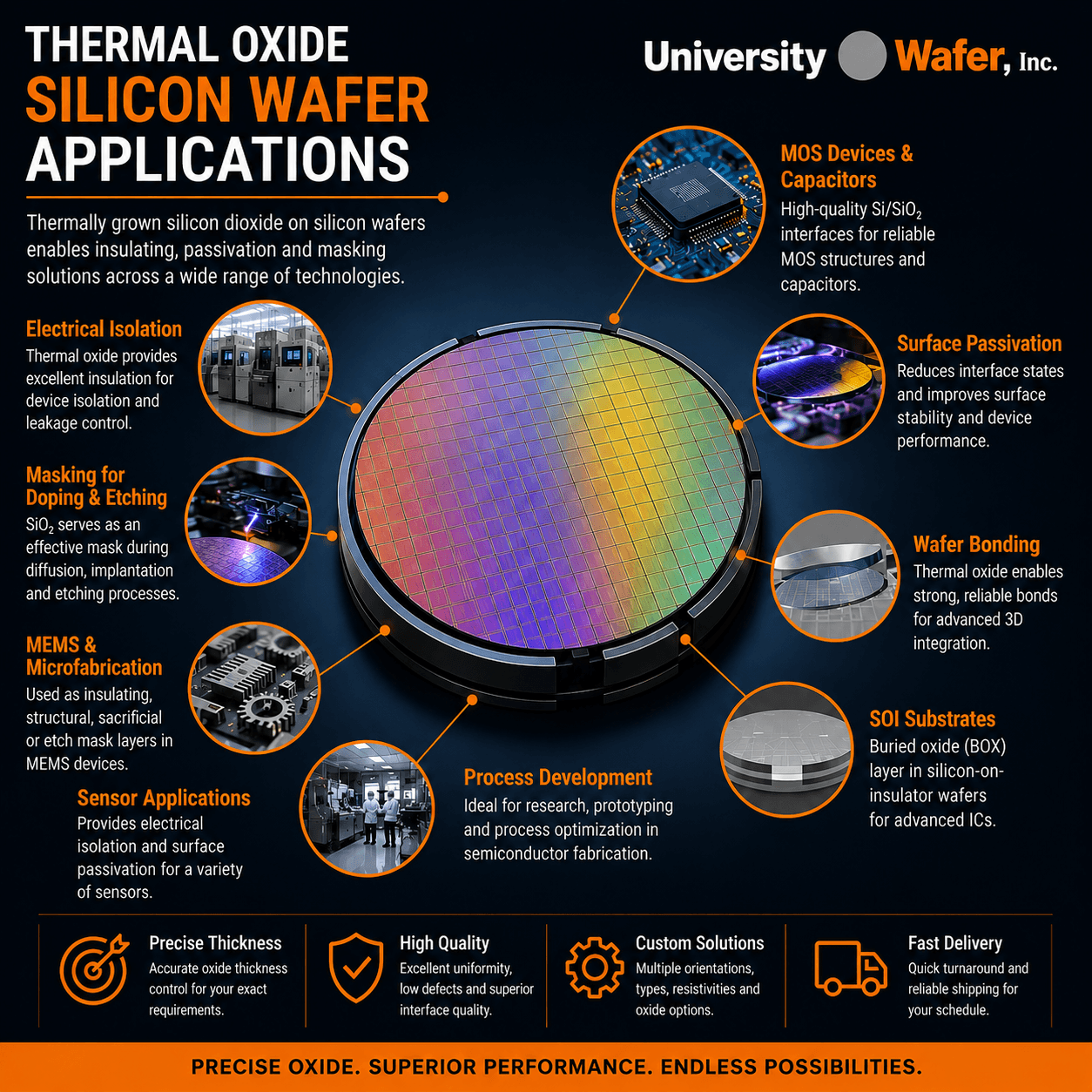
Thermal Oxide Wafer Applications
Thermally oxidized silicon is used throughout semiconductor research and microfabrication. The appropriate oxide thickness and substrate specification depend on the intended process.
Electrical Insulation
Silicon dioxide is an electrical insulator and can electrically separate conductive or semiconducting regions from the silicon substrate. Thermal SiO₂ is therefore useful in MOS structures, test devices and numerous microfabrication processes.
MOS Devices and Capacitors
The high-quality Si/SiO₂ interface made thermal oxide historically fundamental to metal-oxide-semiconductor (MOS) technology. Thermal oxide remains useful for MOS capacitors, research structures and many microelectronic processes.
In advanced commercial CMOS technology, however, the primary gate dielectric is not necessarily conventional SiO₂. High-k dielectric materials are used in many modern transistor technologies to achieve greater effective gate capacitance while limiting leakage current.
Surface Passivation
A properly grown oxide can passivate the silicon surface by reducing the density of electrically active interface states associated with unsatisfied silicon bonds. Surface and interface quality are important in many electronic, sensor and research applications.
Masking During Semiconductor Processing
SiO₂ can be used as a masking material during selected diffusion, etching and ion-implantation processes. The effectiveness of an oxide mask depends on oxide thickness, dopant species, implantation energy, temperature and the specific fabrication process.
Because the required stopping or diffusion-barrier capability varies with the process, oxide thickness should be selected according to the actual fabrication conditions rather than assuming that any SiO₂ layer will provide sufficient masking.
MEMS and Microfabrication
In MEMS fabrication , silicon dioxide can function as an electrical insulator, etch mask, sacrificial material or part of a multilayer device structure.
Thermal oxide is particularly useful when a well-controlled SiO₂ layer is required directly on a silicon substrate before subsequent lithography, etching, deposition or bonding processes.
Device Isolation
Thermal oxidation has also been used for electrical isolation between semiconductor devices. One historical example is Local Oxidation of Silicon (LOCOS), in which relatively thick field oxide regions were selectively grown to isolate neighboring devices.
Modern integrated circuits commonly use other isolation technologies, such as shallow trench isolation (STI), but LOCOS remains important in the history and study of semiconductor processing.
Wafer Bonding and Research Structures
Oxidized silicon wafers are also useful in wafer bonding experiments, dielectric-stack development, thin-film research and the fabrication of specialized structures where a controlled insulating layer is required between silicon and another material.
Silicon dioxide is also an important component of silicon-on-insulator (SOI) structures, where a buried oxide (BOX) electrically isolates a thin silicon device layer from the underlying silicon handle wafer.
Thermal Oxide Thickness
Oxide thickness is one of the most important specifications when selecting a thermal oxide wafer. The required thickness depends on whether the oxide will be used for electrical isolation, masking, optical experiments, microfabrication, surface passivation or another purpose.
UniversityWafer can supply thermally oxidized silicon substrates across a range of oxide thicknesses. Availability depends on the requested wafer diameter, silicon specification, oxide thickness and quantity.
When requesting a quote, specify the desired SiO₂ thickness in nanometers (nm), micrometers (µm), or angstroms (Å), together with the acceptable thickness tolerance.
Thermal Oxide on One Side or Both Sides
Depending on the oxidation process and masking configuration, oxide may be required on one or both wafer surfaces. For many furnace oxidation processes, exposed silicon surfaces oxidize wherever they contact the oxidizing ambient.
If your experiment specifically requires oxide on only one side, or requires different frontside and backside conditions, include that requirement when requesting a quotation.
Thermal Oxide vs. Deposited SiO₂
Thermal oxidation and oxide deposition both produce SiO₂-containing films, but they are fundamentally different processes.
Thermal oxide is grown by chemically converting the surface of a silicon substrate into SiO₂. This produces an oxide with an excellent interface to the underlying crystalline silicon.
Deposited oxide is added to the surface rather than grown by consuming silicon. Deposition techniques can include chemical vapor deposition (CVD), plasma-enhanced chemical vapor deposition (PECVD) and processes using tetraethyl orthosilicate (TEOS) as a precursor.
Deposited oxide can be advantageous when oxidation temperatures are incompatible with the process, when SiO₂ must be formed over materials other than silicon, or when the required film structure cannot be produced conveniently by thermal oxidation.
The best choice therefore depends on the required interface quality, thickness, thermal budget, substrate material and downstream processing.
Choosing a Thermal Oxide Silicon Wafer
Oxide thickness alone is not enough to fully specify an oxidized wafer. The properties of the underlying silicon can be just as important to the experiment or fabrication process.
Useful specifications to provide include:
- Wafer diameter
- Thermal oxide thickness and tolerance
- Dry or wet oxide, when required
- Oxide on one side or both sides
- Crystal orientation, such as <100> or <111>
- P-type or N-type conductivity
- Dopant species
- Resistivity range
- Silicon wafer thickness
- Single-side-polished (SSP) or double-side-polished (DSP)
- Prime, test or other required wafer grade
- Quantity
Providing complete specifications makes it easier to identify an available substrate or determine whether custom oxidation is appropriate for the application.
Why Use Thermally Oxidized Silicon?
Thermally grown SiO₂ remains one of the most useful materials in silicon processing because it combines electrical insulation, chemical stability, compatibility with lithographic processing and a high-quality interface with crystalline silicon.
These characteristics make oxidized silicon wafers useful for university research, semiconductor process development, MEMS, MOS structures, dielectric studies, wafer bonding and many other microfabrication applications.