
We typically use samples grown on your GaAs wafers, but I am working on
a project which will require a transparent substrate (at 780nm). I'm
sure that no one makes AlGaAs wafers to replace the GaAs, but I was
wondering if you know of someone that grows moderately thick (~50-100
um) layers of AlGaAs on your GaAs wafers. Can you prepare something
like that at University Wafer?
AlGaAs Substrates to Replace GaAs
A graduate student requested a quote for the following .
UniversityWafer, Inc. replied:
Yes, we can grow AlGaAs on GaAs although layers as thick as 50 or 100um would get expensive.
However, to start with, what ratio of Al to Ga (on mole basis) do you want? Al50%Ga50%As and even Al90%Ga10%As is possible. What %Al do you want?
Reference #133438 for specs and pricing.
Get Your Quote FAST! Or, Buy Online and Start Researching Today!
AlGaAs Wafers for Research
A PhD student requested a quote for the following.
Question:
I am wondering do you have AlGaInP or AlGaAs wafers? I know it's hard to get those kind of wafers, but I still want to make a try.
Answer:
We can make each of AlGaAs, InGaP and AlGaP but as MOCVD Epi layers. Because of inherent lattice mismatch to a substrate and consequent stresses one can do this either for small % alloys, or for very thin Epi layers (up to about 50nm). If you specify what you want then we can make the required wafers but understand that such wafers cost somewhere between expensive.
Reference #114340 for specs and pricing.
Silicon Disks for AlGaAs Bonding
A photonics researcher requested a quote for the following.
We are looking for thin (< ~ 200 um) silicon disks and I have some questions: 1. What is the highest n-type doping level that can be made? 2. What is the ohmic resistance at such a doping level? 3. Can you make ohmic contacts on both sides of the disk? 4. How thin can these disks be made? 200 um is probably ok for us, but it depends on the resistance (question 2).
Basically, we are trying to bond an AlGaAs chip to a small and thin piece of silicon disk. Then, on the other side of the silicon disk, we want to bond it to a copper or steel block. Can silicon wafers be coated with AuZn or any material that solder can stick?
The reason why we want to have a piece of silicon between the AlGaAs and the metal (copper or steel) is that silicon has a thermal expansion coefficient quite close to AlGaAs. We do not want to use conductive epoxy, because we worry about the reliability for high-current (peak current 3-5 A) operation. The reason for using a thin silicon disk is to minimize ohmic resistence.
Reference #117931 for specs and pricing.
What Are AlGaAs Epitaxial Layers on GaAs?
Aluminum gallium arsenide (AlGaAs, AlxGa1−xAs) is a III–V semiconductor alloy most often used as an epitaxial layer grown on gallium arsenide (GaAs) wafers, rather than as a conventional bulk AlGaAs substrate. AlGaAs/GaAs heterostructures let researchers tailor bandgap and carrier confinement for optoelectronic and electronic devices. The alloy composition, film thickness, doping, and substrate properties depend on the intended device.
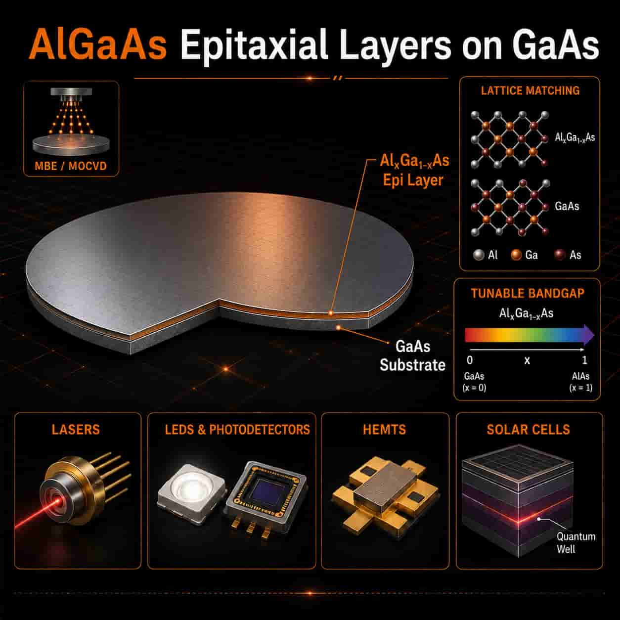
Key Properties of AlGaAs:
- Bandgap Tunability: The bandgap of AlGaAs can be engineered by adjusting the Al/Ga ratio, allowing for better design flexibility in optoelectronic devices.
- High Electron Mobility: Offers good transport properties, making it suitable for high-speed electronic applications.
- Composition-Dependent Bandgap: AlGaAs has a direct bandgap at lower aluminum fractions and becomes indirect at higher aluminum fractions; the composition should match the optical device design.
- Lattice-Matched to GaAs: AlGaAs can be grown epitaxially on GaAs substrates without introducing significant defects, making it ideal for heterostructure devices.
Applications of AlGaAs Substrates:
- Laser Diodes: Used in infrared and visible lasers, such as those in CD/DVD/Blu-ray drives, laser pointers, and fiber-optic communication systems.
- Light-Emitting Diodes (LEDs): Used in high-efficiency LEDs, particularly in the infrared and red wavelength range.
- High-Electron-Mobility Transistors (HEMTs): Found in RF and microwave applications, including satellite communications and radar.
- Photodetectors & Solar Cells: AlGaAs-based detectors are used in infrared sensing, while AlGaAs/GaAs heterojunctions are used in high-efficiency solar cells.
- Quantum Well & Superlattice Structures: Used in research and advanced semiconductor applications, including quantum cascade lasers.
- Electro-Optic Modulators: Used in optical communication systems for high-speed signal processing.
AlGaAs is typically grown using epitaxial methods such as Molecular Beam Epitaxy (MBE) or Metal-Organic Chemical Vapor Deposition (MOCVD) on GaAs wafers. If you are looking for AlGaAs substrates for a specific application, let me know the details, and I can suggest suitable options.
AlGaAs/GaAs Epitaxial Wafer Specifications for a Quote
For a custom AlGaAs on GaAs epitaxial wafer, specify the application and target wavelength (for example, 780 nm or 850 nm), aluminum mole fraction, GaAs wafer diameter and orientation, epi-layer thickness, doping type and concentration, layer sequence, quantity, and any characterization requirements. The requested layer stack should be evaluated for strain, growth feasibility, and device performance.
AlGaAs layers may be used for quantum wells, laser cladding and barriers, photodetectors, and semiconductor heterostructures. Explore III–V semiconductor materials and epitaxially grown device structures when defining your requirements.
AlGaAs 850 nm Epitaxial Wafer Research Specifications
A materials scientist requested a quote for the following.
Our application is as below, pls quote your related epi wafer.
Our 850nm photo diode is from AlGaAs/AlGaAs epi wafer, the structure is DDH, can support high
power output and high speed modulation
Below is application drawing for reference:
| Parameter | Symbol | Condition | Min. | Typ. | Max. |
|---|---|---|---|---|---|
| Forward voltage | VF | IF = 50mA | - | 1.54V | 1.80V |
| IF = 50mA | - | 1.98V | 2.50V | ||
| Reverse voltage | VR | IR = 10μA | 5V | - | - |
| Wavelength | λp | IF = 50mA | - | 850nm | - |
| Spectral width at half height | ∆λ | IF = 50mA | - | 35nm | - |
| Radiant power | P0 | IF = 20mA | 1.00mW | 1.80mW | - |
| Rise / Fall time | Tr/Tf | IF = 50mA | - | 25/15ns | 35/35ns |
UniversityWafer, Inc. Replied:
We are able to make AlGaAs/AlGaAs epi wafers, both 2" and 3" diameter. We do this by MOCVD.
We do not know what you mean by "the structure is DDH". You have to describe to us what structure you require.
Your specification of the structure must include the thickness and composition of each Epi layer, and its degree of doping.
We can guarantee that the Epi wafers structure, that we produce, has Epi layers, each of specified thickness, composition and doping. We can adjust Epi composition to meet specified emission wavelength and produce measurements of emission wavelength at each point on the wafer. However, it is the client's responsibility to verify that the specified structure yields LED parameters that you specified.