Can you please send me a quote for Alpha quartz substrates for film growth and implanting ions.
Size: 2 cm X 2 cm X 1 mm - 2 mm
Quantity: 20 Pcs
UniversityWafer supplies single-crystal alpha quartz wafers in AT-cut, ST-cut, X-cut, Y-cut and Z-cut orientations for piezoelectric sensors, QCM and SAW devices, optical research, photolithography and thin-film experiments. Custom diameters, thicknesses, polished finishes and crystal orientations are available for university, government and industrial laboratories.

Alpha quartz substrates can support specialized thin-film growth, implantation and materials-characterization research. A postdoctoral researcher requested the following custom configuration:
Can you please send me a quote for Alpha quartz substrates for film growth and implanting ions.
Size: 2 cm X 2 cm X 1 mm - 2 mm
Quantity: 20 Pcs
Reference #186860 for specs and pricing.
The crystallographic cut affects the optical, acoustic and piezoelectric response of quartz. UniversityWafer can help identify X-cut, Y-cut or Z-cut quartz wafers from a previous order or source a custom orientation. A university professor requested:
I am doing some experiments on Quartz and the wafers have been purchased from your company couple of years ago.
They are 25 wafers of Quartz, Single Side Polish, 3" and 350um thick. I need to know the structure (alpha or beta quartz) and cut of the wafers (x, y or z). I couldn't find this information on the website and appreciate if you can help me with it.
Reference #116061 for specs and pricing.
Request an alpha quartz wafer quote. Send the cut, diameter or shape, thickness, polish, quantity and application you need, or buy substrates online.
Researchers may compare single-crystal alpha quartz, amorphous silica and polycrystalline quartz to study how crystal structure affects a material or process. A university PhD researcher requested:
"For an experiment, I need to order the following:
None of these items need to be polished. Ideally -- I'm looking for small discs or squares of each of these samples, ~5mm diameter, 250 discs of each type.
But, if it is less expensive to purchase these quartz samples as much larger wafers from you then we can work with that as well. Also if you only sell these items thicker than 50 microns, that's okay, we can have them lapped." Please let me know if you need any more information to offer these.
Reference #137647 for specs and pricing.
I’m wanting to purchase quartz wafers from your company for a chemical vapor deposition (CVD) system which is used to make graphene on copper foil. I was hoping to put the wafers on the quartz boat (where the copper is placed), at the front and back of the boat, so I can analyze particles on the quartz wafers after the CVD process and check for residual contaminants.
Question:
Would you recommend any specific type of quartz wafers for this application? After a few runs I’m going to analyse the quartz wafers by SEM, EDX etc.
Answer:
The single Alpha Quartz crystal will have phase transition @ 572° C ( change to Beta Quartz).
What is the temperature unit below °C or ° F?
Reference #162264 for specs and pricing.
Quartz-based photomasks are produced through precision polishing, opaque-film deposition, photoresist coating, lithographic patterning and inspection. High-purity fused silica is commonly used for photomask blanks, while crystalline alpha quartz may be selected for specialized optical and research applications. The correct material depends on wavelength, birefringence, flatness and thermal requirements.
Material: High-purity fused silica or specialty crystalline quartz is selected according to wavelength, birefringence and tool requirements.
Blank preparation: The substrate is formed, annealed or grown using a process appropriate to the selected quartz material.
Cutting: The blank is sliced or diced to the required mask dimensions and thickness.
Orientation: When crystalline quartz is used, its cut and optical axis must match the application.
Lapping: The rough wafer surface is mechanically ground to achieve uniform thickness.
Polishing: Surfaces are polished to the flatness, parallelism and scratch-dig specification required by the lithography process.
Cleaning: Ultrasonic and chemical cleaning remove any residues or particles.
Sputtering or Evaporation: A thin layer (~100 nm) of chrome (Cr) is deposited onto one side of the quartz wafer. Chrome provides the opaque layer necessary for photomask patterning.
Adhesion Layer (optional): A very thin layer of chromium oxide or another adhesive is sometimes applied to improve chrome adhesion to quartz.
A layer of photoresist is spin-coated over the chrome surface.
This layer is sensitive to UV light and will define the circuit pattern.
Exposure: The photoresist-coated substrate is exposed to UV light through a master pattern (reticle).
Development: The exposed or unexposed regions (depending on resist type) are dissolved away, revealing parts of the chrome layer underneath.
Wet or Dry Etch: The exposed chrome areas are chemically etched away, leaving behind the chrome pattern corresponding to the desired circuit design.
The remaining photoresist is stripped, leaving behind a clean chrome-on-quartz circuit pattern.
Flatness, line width accuracy, and optical transmission (>90% UV-Vis) are rigorously tested.
Defect inspection ensures no particles, pits, or pattern errors are present.
The photomask is cleaned again and then sealed in a cleanroom-safe container for delivery or integration into lithographic tools.
Need a quartz substrate for a photomask or lithography experiment? Specify the wavelength, blank size, thickness, flatness, surface quality and coating requirements when requesting a quote.
Alpha quartz (α-quartz) is the stable, low-temperature crystalline form of silicon dioxide (SiO₂). Its ordered crystal structure gives it direction-dependent optical, elastic and piezoelectric behavior. Above approximately 573°C at atmospheric pressure, alpha quartz undergoes a reversible transition to beta quartz.
Alpha quartz is crystalline and piezoelectric; fused silica is amorphous and is selected for many UV, optical and photomask applications. Choosing between them depends on the required crystal response, transmission range, thermal behavior and fabrication process.
Chemical formula: SiO₂
Crystal Structure: Trigonal/hexagonal lattice
Thermal Stability: Stable below 573°C, above which it transitions to β-quartz
Piezoelectric Effect: Exhibits piezoelectric properties (generates electric charges under mechanical stress)
Alpha quartz is an electrical insulator rather than a semiconductor. Its combination of optical transparency, piezoelectric response, chemical stability and low dielectric loss makes it useful in selected semiconductor, RF, acoustic and materials-research workflows.
Quartz substrates (often fused silica or crystalline α-quartz) are widely used in semiconductor processing, especially for photolithography masks, optical elements, and high-frequency RF/Microwave devices due to low dielectric loss, high optical transparency, and dimensional stability.
Alpha quartz is essential for quartz crystal resonators used as oscillators in semiconductor-based electronics. Due to its piezoelectric nature, it precisely controls frequency generation in clocks, microprocessors, radio transmitters, and other timing-critical semiconductor circuits.
Alpha quartz is chemically inert and has minimal thermal expansion, making it ideal for semiconductor processing tools, masks, and equipment components exposed to harsh fabrication conditions (such as plasma etching, deposition, and high-temperature treatments).
Alpha quartz substrates can support thin-film deposition and materials growth experiments involving graphene, carbon nanotubes, III-V semiconductors and metal-oxide materials. The correct surface finish, orientation and thermal budget depend on the deposition process.
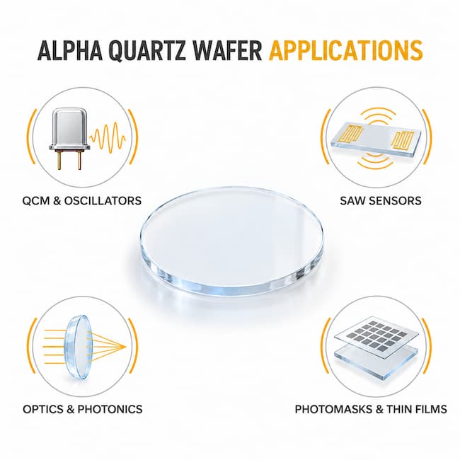
Alpha quartz wafers are used in frequency-control components, QCM, SAW devices, piezoelectric sensors, optical experiments, thin-film deposition and specialized photolithography research. Review our single-crystal quartz wafer guide to compare AT-, ST-, X-, Y- and Z-cut material.