
AFM Surface Characterization of Silicon Wafers
Atomic Force Microscopy (AFM) is a powerful surface-characterization technique used to examine materials at the micro- and nanoscale. By scanning a sharp probe across a sample, AFM can generate detailed three-dimensional information about surface topography, roughness, particles, defects, thin films, and other nanoscale features.
High-quality silicon wafers provide a useful substrate for AFM research because polished silicon surfaces can offer low roughness, excellent flatness, and a well-defined starting surface for experiments involving coatings, nanoparticles, thin films, polymers, biological materials, and semiconductor structures.
How Does Atomic Force Microscopy Work?
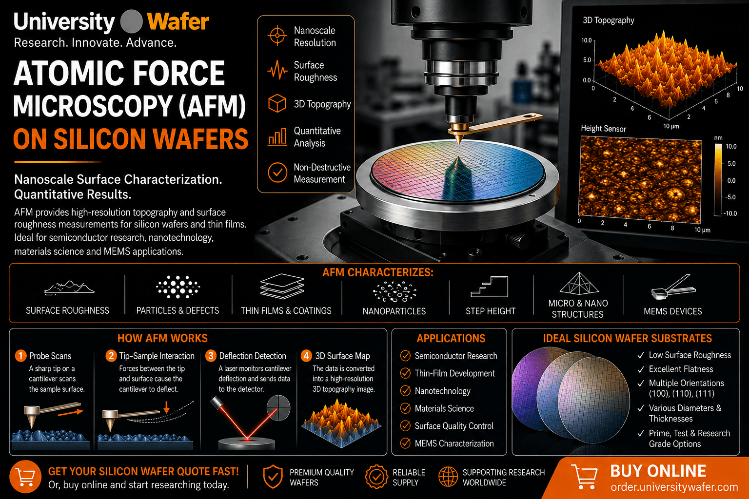
An Atomic Force Microscope uses a very small probe positioned at the end of a flexible cantilever. As the probe scans across the sample, interactions between the tip and surface cause changes in the cantilever's motion or deflection.
The instrument monitors these changes while moving the probe across the selected scan area. The resulting data can be converted into a high-resolution map of the sample surface, allowing researchers to investigate nanoscale variations in height and morphology.
Why Use Silicon Wafers for AFM?
Silicon provides a stable and highly characterized substrate for surface-science experiments. Polished wafers can have very smooth surfaces, making it easier to distinguish deposited materials or experimental features from the underlying substrate.
Researchers requiring especially smooth substrates can use low surface roughness silicon wafers for AFM, nanotechnology, thin-film deposition, wafer bonding, and other applications where nanoscale surface quality is important.
Measuring Silicon Wafer Surface Roughness
One of the most common applications of AFM is surface roughness measurement. Instead of relying only on optical inspection, AFM measures vertical variations across a small surface area and creates quantitative topographical data.
Depending on the analysis software and measurement objective, researchers may evaluate parameters such as average roughness, RMS roughness, peak-to-valley variation, and the distribution of surface features.
AFM Surface Topography
AFM topography allows researchers to visualize the three-dimensional morphology of a silicon wafer or material deposited on its surface. Features such as islands, grains, pits, scratches, particles, steps, and patterned structures can potentially be distinguished within an appropriate scan range.
Because AFM measures surface height directly, it is particularly useful when researchers need quantitative information about nanoscale features rather than only a conventional microscope image.
Contact Mode AFM
In contact mode AFM, the probe remains in continuous interaction with the sample surface while scanning. Changes in cantilever deflection are used to track the topography.
Contact mode can provide useful surface information, but the interaction between the probe and sample should be considered when studying soft coatings, loosely attached particles, or delicate nanoscale structures.
Tapping Mode AFM
Tapping mode AFM operates by oscillating the cantilever so that the tip interacts intermittently with the surface. This can reduce lateral forces compared with continuous contact scanning.
Tapping mode is commonly considered for samples containing delicate structures, thin films, polymers, nanoparticles, and other materials where minimizing tip-sample interaction is desirable.
Non-Contact AFM
In non-contact AFM, the probe operates without maintaining continuous mechanical contact with the sample. The system detects interactions between the tip and surface while the cantilever oscillates near the sample.
The most appropriate AFM mode depends on the material, surface condition, required resolution, environmental conditions, and information being investigated.
AFM Analysis of Thin Films
AFM is frequently used to characterize thin films deposited on silicon wafers. Researchers can investigate how deposition conditions influence surface morphology, grain structure, roughness, particle formation, and other nanoscale characteristics.
Silicon substrates provide a convenient starting platform for depositing metals, dielectrics, semiconductors, oxides, polymers, and other experimental materials.
Researchers requiring oxide-coated substrates can also explore thermal oxide silicon wafers for dielectric, thin-film, MEMS, and surface-characterization research.
AFM for Nanoparticle Research
Silicon wafers can be used as substrates for depositing nanoparticles before AFM characterization. The smooth underlying surface can help researchers identify individual particles, aggregates, surface coverage, and changes in morphology.
This approach can support research involving nanomaterials, catalysts, coatings, colloidal particles, quantum structures, and other nanoscale systems.
Detecting Particles and Surface Defects
AFM can reveal small particles and surface features that may be difficult to characterize using conventional optical microscopy. This makes the technique useful for studying contamination, polishing defects, scratches, pits, deposited particles, and other localized surface features.
Understanding these features can be important when evaluating substrate quality or investigating how wafer preparation affects subsequent semiconductor processes.
AFM for Step-Height Measurements
AFM can also measure vertical differences between adjacent surface regions. This capability makes it useful for analyzing nanoscale step heights, patterned films, etched structures, and deposited layers.
Step-height analysis can complement other surface measurement techniques when researchers require localized measurements at micro- or nanoscale dimensions.
Preparing Silicon Wafers for AFM
Surface preparation is important because contamination can appear prominently in an AFM scan. Dust, residues, fingerprints, water marks, and other unwanted material can be mistaken for actual sample features.
Researchers should use an appropriate silicon wafer cleaning process before AFM analysis when the experiment requires a clean substrate surface.
Additional information about contamination removal and substrate preparation is available in our guide to wafer surface cleaning .
Ultrasonic Cleaning Before AFM
For appropriate samples, ultrasonic cleaning may help remove loosely attached particles and residues before surface characterization. Acoustic energy transmitted through a cleaning liquid can assist with contaminant removal without manually scrubbing the polished wafer surface.
Learn more about ultrasonic wafer cleaning and the role of cavitation, frequency, cleaning chemistry, temperature, and process time in substrate preparation.
AFM and Silicon Wafer Orientation
Silicon wafers are available in crystallographic orientations such as (100), (110), and (111). Orientation can influence surface structure, etching behavior, oxidation, epitaxial growth, and other semiconductor processes.
When AFM is being used to investigate a process that depends on crystal orientation, researchers should select the silicon substrate according to the requirements of the experiment rather than treating all polished silicon surfaces as equivalent.
AFM for MEMS and Microfabrication
Atomic Force Microscopy can also support MEMS research by providing localized surface measurements of fabricated structures, deposited films, etched regions, and other micro- or nanoscale features.
AFM measurements can complement optical microscopy, profilometry, SEM, and other characterization methods used during microfabrication research.
AFM for Semiconductor Research
Atomic Force Microscopy is useful across many areas of semiconductor and materials science, including:
- Silicon wafer surface roughness measurements
- Nanoscale surface topography
- Thin-film morphology
- Particle and contamination analysis
- Nanoparticle characterization
- Step-height measurements
- Surface defect analysis
- MEMS characterization
- Nanotechnology research
- Semiconductor process development
Selecting Silicon Wafers for AFM
The appropriate substrate depends on what the AFM experiment is intended to measure. Researchers should consider specifications such as:
- Wafer diameter
- Crystal orientation
- Surface roughness
- Single-side or double-side polish
- Wafer thickness
- Resistivity and conductivity type
- Native or thermal oxide requirements
- Surface cleanliness
- Prime, test, or research-grade material
Silicon Wafers for AFM Research
UniversityWafer supplies silicon wafers for Atomic Force Microscopy (AFM) and other surface-science applications. Selecting a smooth, clean, and properly specified silicon substrate provides researchers with a controlled starting surface for nanoscale measurements and materials characterization.
Get Your Silicon Wafer for AFM Quote FAST! Or, buy online and start researching today!
AFM Measurement, Surface Roughness and Nanoscale Analysis
Atomic Force Microscopy (AFM) provides researchers with quantitative information about silicon wafer surfaces at extremely small scales. Unlike conventional optical imaging, AFM uses the interaction between a sharp probe and the sample to construct a three-dimensional representation of surface topography.
The technique is particularly useful for analyzing low surface roughness silicon wafers , thin films, coatings, nanoparticles, patterned structures, and other samples where nanoscale variations in height and morphology are important.
AFM Resolution on Silicon Surfaces
AFM can resolve extremely small surface features because the measurement is performed using a nanoscale probe rather than visible light. The achievable resolution depends on the AFM system, probe geometry, scan conditions, sample characteristics, vibration control, and selected imaging mode.
Vertical sensitivity can be especially valuable when researchers need to distinguish subtle differences in surface height, roughness, or deposited material on a polished silicon substrate.
Understanding AFM Surface Roughness
AFM surface roughness measurements provide quantitative information about variations in surface height within a selected scan area. Roughness values should always be interpreted together with scan dimensions, sampling conditions, data processing, and the condition of the AFM probe.
This is particularly important when comparing different silicon wafer surfaces or evaluating how cleaning, polishing, oxidation, deposition, etching, or other processes affect surface morphology.
Ra and RMS Roughness
Two commonly reported surface parameters are average roughness (Ra) and root-mean-square roughness (Rq or RMS). Both describe variations in surface height, but they calculate those variations differently.
RMS roughness gives greater mathematical weight to larger deviations from the mean surface level. For meaningful comparisons, researchers should use consistent scan sizes, processing methods, and measurement conditions.
AFM Scan Size Matters
The selected AFM scan area can strongly influence the resulting roughness measurement. A very small scan may reveal atomic-scale or nanoscale morphology, while a larger scan can capture particles, scratches, grains, or other features distributed across a broader region.
For this reason, a roughness value without information about scan dimensions may provide an incomplete description of the silicon wafer surface.
AFM Cantilevers and Probe Selection
The AFM cantilever and tip should be selected according to the sample and imaging mode. Parameters such as cantilever stiffness, resonance frequency, tip radius, probe coating, and geometry can influence measurement performance.
A probe appropriate for a hard polished silicon surface may not necessarily be optimal for a soft polymer film, loosely attached nanoparticles, biological material, or another delicate sample.
AFM Tip Geometry and Image Quality
The shape of the AFM tip influences how accurately the instrument reproduces surface features. Because the probe has a finite radius, narrow trenches, steep sidewalls, and very small particles can appear different from their actual geometry.
Researchers should therefore consider tip convolution when interpreting the lateral dimensions of nanoscale features. A worn or contaminated probe can also introduce artifacts and reduce measurement reliability.
Recognizing AFM Imaging Artifacts
Not every feature visible in an AFM image necessarily originates from the sample. Common sources of artifacts can include:
- Contaminated or damaged AFM tips
- Vibration and acoustic noise
- Thermal drift
- Improper feedback settings
- Excessive scan speed
- Tip-sample interaction
- Surface contamination
- Data-processing effects
Repeating measurements at different locations, changing scan direction, or replacing the probe can help determine whether an unusual feature belongs to the sample or is associated with the measurement process.
AFM Analysis of Polished Silicon Wafers
Polished silicon provides a useful reference surface for nanoscale characterization because its morphology can be significantly smoother than many deposited or processed materials.
Researchers interested specifically in surface-sensitive experiments can use silicon wafers for AFM research as substrates for thin films, nanoparticles, coatings, nanostructures, and surface-science experiments.
AFM Analysis Before and After Wafer Cleaning
AFM can help researchers compare silicon surfaces before and after cleaning. Changes in particle density, residue, morphology, or measured roughness can provide information about how a cleaning procedure affects the substrate.
UniversityWafer provides additional information about silicon wafer cleaning and wafer surface preparation for semiconductor and materials research.
Ultrasonic Cleaning and AFM Samples
Particles and residues can significantly influence nanoscale surface measurements. For suitable samples, ultrasonic wafer cleaning may be used as part of a substrate-preparation procedure before AFM characterization.
However, ultrasonic cleaning parameters should be selected carefully when samples contain delicate thin films, nanoparticles, membranes, patterned structures, or other features that could be affected by acoustic cavitation.
AFM Characterization of Silicon Oxide
AFM can be used to examine the surface morphology of oxidized silicon substrates and determine how processing affects nanoscale roughness and topography.
Researchers working with dielectric surfaces can explore thermal oxide silicon wafers for thin-film, dielectric, MEMS, semiconductor, and surface-characterization experiments.
AFM for Thin-Film Morphology
A smooth silicon substrate can provide a controlled starting surface for evaluating deposited thin films. After deposition, AFM can reveal changes in morphology that may be associated with nucleation, grain formation, growth conditions, coating thickness, or post-deposition processing.
Materials commonly investigated on silicon substrates can include metals, semiconductor layers, oxides, polymers, nanoparticles, and other experimental coatings.
AFM and Silicon Epitaxial Layers
AFM can also support characterization of silicon epitaxial wafers by providing localized information about surface morphology and roughness after epitaxial growth.
Surface characterization can help researchers investigate how epitaxial conditions, substrate preparation, layer growth, and subsequent processing influence the final wafer surface.
AFM for MEMS Surface Characterization
In MEMS research , AFM can be used to characterize accessible surfaces of deposited films, etched regions, microstructures, and other fabricated features.
Surface roughness can be relevant to mechanical contact, adhesion, friction, coating performance, and other characteristics of microfabricated devices.
AFM and Silicon-on-Insulator Wafers
Researchers working with Silicon-on-Insulator (SOI) wafers may use AFM to investigate the surface of the silicon device layer before or after fabrication.
SOI substrates are widely used for MEMS, photonics, RF, sensors, and advanced semiconductor research where control of the device-layer surface can be important.
AFM vs. Profilometry
AFM and profilometry both measure surface height, but they are useful at different dimensional scales. AFM is particularly valuable for localized nanoscale topography and roughness, while profilometry can be useful for larger scan lengths and step-height measurements.
Using multiple characterization techniques can provide a more complete understanding of surface morphology than relying on a single measurement method.
AFM vs. Scanning Electron Microscopy
AFM and SEM provide complementary information. SEM can produce high-resolution images of surface structures over useful lateral ranges, while AFM directly measures three-dimensional surface topography and does not inherently require the sample to be electrically conductive.
For some experiments, researchers use both techniques to correlate visual morphology with quantitative surface-height measurements.
AFM vs. Optical Microscopy
Optical microscopy is useful for rapidly locating larger particles, scratches, patterned regions, and other visible features. AFM can then examine a selected region at much smaller dimensions and provide quantitative topographical information.
Combining optical inspection with AFM can make it easier to locate representative areas before performing time-intensive nanoscale scans.
AFM Sample Preparation
Proper sample preparation helps improve measurement reliability. Before AFM analysis, researchers should consider:
- Surface cleanliness
- Sample stability and mounting
- Wafer orientation and identification
- Appropriate scan area
- Expected surface roughness
- AFM probe selection
- Imaging mode
- Environmental vibration and contamination
Reporting AFM Results
For reproducible surface characterization, researchers should document the measurement conditions together with the resulting roughness values. Useful information can include AFM mode, scan dimensions, resolution, probe type, scan rate, data-processing method, and the number of locations measured.
This additional information makes it easier to compare results between different wafers, deposition processes, cleaning procedures, and research laboratories.
Choosing Silicon Substrates for AFM Research
UniversityWafer supplies silicon substrates with different diameters, orientations, resistivities, thicknesses, oxide layers, and surface finishes for AFM, nanotechnology, thin-film research, surface science, MEMS, and semiconductor characterization.
For experiments where the substrate itself should contribute minimal nanoscale topography, selecting a high-quality polished low-roughness silicon wafer can provide a controlled starting surface for AFM measurements.
Related Links
- Silicon Wafers for Atomic Force Microscopy (AFM)
- Low Surface Roughness Silicon Wafers
- Silicon Wafers for Research
- Silicon Wafer Cleaning
- Silicon Wafer Surface Cleaning
- Ultrasonic Wafer Cleaning
- Thermal Oxide Silicon Wafers
- Silicon Epitaxial Wafers
- Silicon-on-Insulator (SOI) Wafers
- Wafers for MEMS Research