
Bonded SOI Wafers for Research and Device Fabrication
Bonded SOI substrates provide a defined silicon device layer above an insulating oxide. For MEMS and sensor fabrication, the BOX can act as an etch stop or sacrificial layer, depending on the process. Device layer thickness and uniformity are key selection parameters for structures such as pressure-sensor membranes, accelerometers, and resonators.
Researchers also select SOI for microfluidic devices, SOI transistor research, and optical structures. Each application requires its own layer stack; a thick MEMS device layer and a thin photonic device layer serve different fabrication requirements.
Common SOI Wafer Applications
- MEMS and MST devices
- RF MEMS switches and resonators
- BioMEMS and microfluidic devices
- MOSFET and CMOS research
- Optoelectronic devices
- Smart power devices
- Advanced analog integrated circuits
- Pressure sensors and accelerometers
- Silicon photonics
- Luxury watch components
Get Your Quote FAST! Or, Buy Online and Start Researching Today!
Silicon-on-Sapphire vs SOI Wafers
Silicon-on-sapphire (SOS) wafers use sapphire as the insulating support, while bonded SOI uses buried oxide above a silicon handle. Compare the insulating material, layer thicknesses, thermal requirements, and intended RF or sensor design when selecting between these substrates.
Direct-Bonded SiSi Wafers vs Bonded SOI
Direct-bonded silicon-to-silicon (SiSi) wafers have no buried oxide between the bonded silicon layers. They are distinct from SOI stacks with an insulating BOX layer and can be considered for fast PIN diode research. Specify whether your project requires an oxide-free SiSi interface or an insulating SOI structure when requesting wafer bonding or a bonded substrate quote.
Bonded Silicon-on-Insulator (SOI) Wafers
Bonded SOI wafer selection starts with the device layer, buried oxide, and handle wafer. The top silicon supports the active device or mechanical structure, the BOX provides electrical isolation, and the handle supports the stack. Silicon wafer bonding enables engineered substrate combinations for research and fabrication.
UniversityWafer offers bonded wafer options with a broad range of silicon layer thicknesses, including thin device layers and thick bonded structures. Confirm the required BOX thickness and current availability for your specific SOI stack. The sample inventory below includes both oxide-containing SOI and zero-oxide SiSi bonded wafers.
Available configurations include N-type silicon and P-type silicon layers, with 100 mm, 125 mm, and 150 mm examples shown below. Specify the conductivity type of the device layer and handle separately, together with silicon resistivity and crystal orientation. Contact us about additional diameters and custom SOI specifications.
Contact us with your required device layer thickness, buried oxide thickness, handle wafer specification, orientation, and resistivity for a fast quotation.
Please email us your specs for an immediate quote. Or buy online here:
Sample Bonded Wafer Inventory: SOI and SiSi
Reading the BOX column: Rows with 0 Å list direct-bonded SiSi wafers without an insulating buried oxide. Rows with a nonzero BOX value describe oxide-containing stacks. For comparison, 10,000 Å = 1 µm. Confirm specifications and availability before ordering.
| Diameter | Handle Thickness (µm) | BOX Thickness (Å) | Device Layer (µm) | Device Resistivity | Type |
|---|---|---|---|---|---|
| 100mm | 514 | 0 | 11 | 2500–5500 Ω-cm | N/N |
| 100mm | 505 | 0 | 20 | 2500–5500 Ω-cm | N/N |
| 100mm | 480 | 0 | 45 | 2500–5500 Ω-cm | N/N |
| 100mm | 440 | 0 | 85 | 2800–5200 Ω-cm | N/N |
| 100mm | 637 | 0 | 125 | 2800–5200 Ω-cm | N/N |
| 100mm | 400 | 0 | 175 | >5000 Ω-cm | N/N |
| 100mm | 475 | 0 | 525 | >5000 Ω-cm | N/N |
| 125mm | 550 | 10,000 | 20 | 1–30 Ω-cm | P/P |
| 150mm | 380 | 6,000 | 15 | 0.05–0.1 Ω-cm | N/P |
| 150mm | 573 | 20,000 | 50 | 14.4–17.6 Ω-cm | N/N |
Need a custom SOI wafer? Send your required device layer and tolerance, BOX thickness, handle thickness, doping, resistivity, diameter, orientation, surface finish, and quantity. We can check current inventory and discuss custom bonded wafer options.
How to Choose Bonded SOI Wafer Specifications
- Device layer thickness: Match the top silicon thickness and tolerance to your membrane, resonator, transistor, or optical structure. Specify thickness uniformity across the wafer.
- Buried oxide thickness: State the BOX thickness required for insulation, etch stopping, or release. An oxide-free SiSi wafer cannot provide BOX isolation.
- Handle wafer: Specify support thickness and electrical properties independently from the device layer.
- Doping and resistivity: Select conductivity type and resistivity for both silicon layers. See the silicon resistivity guide for background.
- Orientation and dimensions: Confirm silicon crystal orientation, diameter, flat or notch, and compatibility with your fabrication equipment.
- Surface and flatness: Include polishing requirements, surface roughness, bow, warp, and total thickness variation limits when relevant.
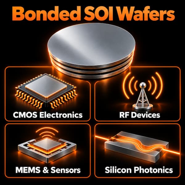
Bonded SOI Wafer Applications: MEMS, Sensors and Photonics
Bonded silicon-on-insulator wafers are used in a wide variety of semiconductor and MEMS applications because of their excellent electrical isolation and reduced parasitic capacitance. The buried oxide layer improves device performance while allowing precise control of the silicon device layer thickness.
- MEMS pressure sensors
- Accelerometers and gyroscopes
- RF MEMS switches and resonators
- Silicon photonics
- BioMEMS and microfluidics
- Power electronics
- Smart power devices
- Advanced analog ICs
- SOI MOSFET fabrication
- Optoelectronic devices
Advantages of Bonded SOI Wafers
Compared with bulk silicon wafers, an SOI stack adds buried oxide isolation and independent control of the device layer. This can reduce parasitic coupling in appropriate device designs and provide an etch stop or release layer for MEMS. Electrical performance depends on the device architecture, layer thicknesses, doping, and fabrication process.
- Excellent electrical isolation
- Device-to-handle isolation through the BOX layer
- Device layer thickness selected for the application
- Engineered substrate options for RF research
- BOX etch-stop and sacrificial-layer options for MEMS
- Precise device layer thickness control
- Separate device and handle layer specifications