
What Is a Bulk Silicon Wafer?
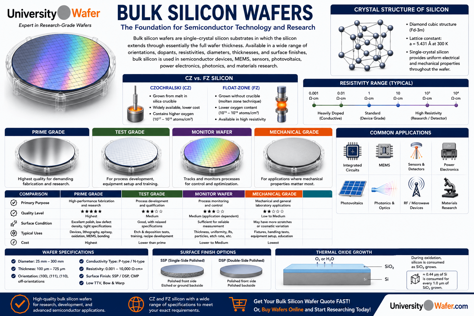
A bulk silicon wafer is a semiconductor substrate composed primarily of crystalline silicon through essentially the full thickness of the wafer. In most semiconductor applications, bulk wafers are cut from single-crystal silicon ingots and subsequently shaped, etched, cleaned, and polished to produce surfaces suitable for device fabrication and materials research.
Bulk silicon differs from engineered layered substrates such as silicon-on-insulator (SOI) wafers , which contain a comparatively thin crystalline silicon device layer separated from a handle substrate by an insulating buried oxide layer. Bulk silicon instead provides a continuous silicon substrate without this intentionally incorporated buried insulating layer.
Silicon wafers are widely used for integrated circuits, discrete semiconductor devices, MEMS, sensors, photovoltaics, microfabrication, thin-film research, and fundamental semiconductor experiments.
Single-Crystal Silicon
Semiconductor-grade bulk silicon wafers are commonly single-crystal, or monocrystalline, silicon. In a single-crystal wafer, the crystal lattice maintains a continuous crystallographic orientation throughout the substrate apart from defects that may be present at low concentrations.
Single-crystal material is important because grain boundaries found in polycrystalline materials can alter electrical transport, diffusion, mechanical behavior, and device uniformity. Controlled crystallographic orientation is also essential for processes whose behavior depends on crystal direction, including anisotropic silicon etching.
Czochralski (CZ) Silicon Wafers
The Czochralski process is one of the principal methods used to manufacture large single-crystal silicon ingots. During Czochralski crystal growth , a seed crystal is brought into contact with molten silicon and then carefully pulled and rotated while the melt solidifies onto the seed.
Control of pulling conditions allows a cylindrical single-crystal ingot to be produced with the desired crystallographic orientation and approximate diameter. Dopants can be introduced into the melt when a specified conductivity type and electrical resistivity are required.
Because conventional CZ growth uses a silica crucible, oxygen can enter the silicon melt and become incorporated into the growing crystal. Oxygen concentration and its subsequent behavior can influence mechanical, defect, and gettering characteristics during later thermal processing.
Float-Zone (FZ) Silicon Wafers
Float-zone silicon is produced without melting the silicon in direct contact with a crucible. A narrow molten zone is passed along a silicon rod, allowing impurities to redistribute as the material recrystallizes.
The absence of a silica crucible generally results in substantially lower oxygen concentrations than conventional CZ silicon. FZ material is also available at high electrical resistivity, making it useful for applications where low free-carrier concentration or low dielectric loss is important.
FZ silicon wafers are used in research involving high-resistivity substrates, detectors, power devices, RF and microwave structures, and other applications requiring particular electrical or impurity characteristics.
CZ Silicon vs. FZ Silicon
Choosing between CZ and FZ silicon depends on the application rather than one growth method being universally superior. Important differences can include oxygen concentration, achievable resistivity ranges, wafer diameter availability, defect behavior, mechanical response during processing, and cost.
- CZ silicon: widely available, suitable for many semiconductor processes, and generally contains more oxygen than conventional FZ silicon.
- FZ silicon: generally has lower oxygen content and is particularly useful when high resistivity or low impurity concentration is required.
The correct material should therefore be selected according to the device, thermal processing sequence, electrical requirements, and research goals.
Silicon Crystal Orientation
A silicon wafer orientation describes how the wafer surface is aligned relative to the silicon crystal lattice. Common orientations include (100), (111), and (110), although other orientations and intentional off-axis cuts can be supplied for specialized applications.
Crystal orientation can influence oxidation kinetics, surface atomic structure, carrier behavior, epitaxial growth, cleavage, and wet-etching characteristics. Orientation is therefore an important specification rather than simply a geometric description of the wafer.
For example, anisotropic silicon etching exploits the different etch rates of crystallographic planes in single-crystal silicon. This behavior is widely used in MEMS and microfabrication.
P-Type and N-Type Bulk Silicon
Pure silicon can be intentionally doped to control its electrical conductivity. Adding electrically active impurities changes the equilibrium concentrations of electrons and holes and allows silicon wafers to be produced with specified conductivity type and resistivity.
P-type silicon is commonly produced using acceptor dopants such as boron. In p-type material, holes are the majority carriers under ordinary equilibrium conditions.
N-type silicon can be produced using donor dopants such as phosphorus, arsenic, or antimony. In n-type material, electrons are the majority carriers.
Conductivity type and doping concentration are important when bulk silicon is used for semiconductor junctions, MOS structures, detectors, sensors, power devices, and other electronic applications.
Silicon Wafer Resistivity
Silicon resistivity, commonly specified in ohm-centimeters (Ω·cm), describes the material's resistance to electrical current flow for a defined geometry. In doped silicon, resistivity depends strongly on carrier concentration and carrier mobility, both of which depend on dopant concentration and temperature.
Heavier electrically active doping generally lowers resistivity, although the relationship is not simply linear because carrier mobility also changes with doping concentration.
Researchers requiring very conductive substrates may use heavily doped silicon wafers , while high-resistivity silicon can be selected for applications requiring reduced substrate conduction.
High-Resistivity Bulk Silicon
High-resistivity silicon wafers are important for applications where electrical conduction through the substrate should be minimized. Depending on material quality, compensation, growth method, and doping, bulk silicon can be produced with substantially higher resistivity than conventional device-grade doped wafers.
High-resistivity silicon is used in areas such as radiation detectors, RF and microwave research, high-voltage structures, photonics, and specialized sensor development. Float-zone silicon is frequently selected for these applications because very high resistivity and low oxygen concentration can be achieved.
Polished Silicon Wafer Surfaces
After an ingot is sliced, a silicon wafer undergoes several mechanical and chemical processing steps before it is suitable for many semiconductor applications. These can include edge shaping, lapping or grinding, chemical etching, cleaning, and chemical mechanical polishing (CMP) .
Polishing produces a smooth surface appropriate for processes such as photolithography, oxidation, thin-film deposition, epitaxy, bonding, and device fabrication.
Bulk silicon wafers may be supplied as single-side polished (SSP) or double-side polished (DSP), depending on whether one or both wafer surfaces require a high-quality polished finish.
Epi-Ready Bulk Silicon Substrates
Bulk silicon can also serve as a starting substrate for silicon epitaxial growth . Epitaxy forms a crystalline layer with a defined crystallographic relationship to the underlying substrate.
An epi-ready wafer requires appropriately controlled surface cleanliness, roughness, crystallographic quality, and handling so that it can support subsequent epitaxial processing. The substrate and epitaxial layer can have different doping levels or other engineered properties depending on the intended device.
Bulk Silicon Wafer Specifications
Selecting the correct bulk silicon substrate requires more than choosing a wafer diameter. Specifications that may be important include:
- Crystal growth method: CZ or FZ
- Crystal orientation: (100), (111), (110), or another cut
- Conductivity type: p-type or n-type
- Dopant species
- Electrical resistivity
- Wafer diameter and thickness
- Single-side or double-side polishing
- Surface roughness and cleanliness
- Total thickness variation (TTV)
- Bow and warp requirements
- Orientation tolerance or off-cut angle
UniversityWafer supplies bulk silicon wafers for semiconductor fabrication, MEMS, microelectronics, sensors, photovoltaics, thin-film deposition, epitaxial growth, university laboratories, and materials research.
Get Your Bulk Silicon Wafer Quote FAST!
Or,
Buy Wafers Online
and Start Researching Today!
Bulk Silicon for Semiconductor Device Fabrication
Bulk silicon wafers provide the starting substrate for a wide range of semiconductor devices and research processes. Their electrical, crystallographic, mechanical, and surface properties can be selected according to the requirements of the device being fabricated.
In conventional silicon processing, device structures can be formed directly in or on the bulk substrate using processes such as oxidation, doping, photolithography, etching, thin-film deposition, annealing, and metallization. Learn more about these steps in semiconductor device manufacturing .
Bulk silicon is used in integrated-circuit research, discrete devices, sensors, MEMS, photovoltaics, power electronics, photonics, and many experimental semiconductor structures.
Bulk Silicon vs. Silicon-on-Insulator (SOI)
Bulk silicon and silicon-on-insulator (SOI) wafers have fundamentally different substrate structures. In a conventional bulk wafer, crystalline silicon extends through essentially the full substrate thickness. An SOI wafer instead contains a comparatively thin crystalline silicon device layer separated from a handle substrate by an insulating layer, commonly a buried silicon dioxide layer called the buried oxide (BOX).
The buried oxide provides electrical isolation between the device layer and the handle wafer. This can reduce substrate coupling and parasitic capacitances in appropriately designed devices, while also enabling specialized MEMS, RF, photonic, and electronic structures.
Bulk silicon remains appropriate when a buried insulating layer is not required and can offer simpler substrate structures and broad compatibility with established silicon fabrication processes. The correct choice depends on device architecture rather than one substrate being universally superior.
Bulk Silicon vs. Epitaxial Silicon Wafers
A bulk silicon wafer can also be used as the supporting substrate for an epitaxially grown crystalline layer. In a silicon epitaxial wafer , the epitaxial layer has a defined crystallographic relationship with the underlying single-crystal silicon.
The epitaxial layer and bulk substrate can be engineered with different doping concentrations or conductivity characteristics. This allows the near-surface device region to be optimized separately from the mechanical and electrical properties of the underlying wafer.
Epitaxial structures are used in numerous semiconductor technologies, including power devices, integrated circuits, sensors, and other devices requiring controlled near-surface material properties.
Thermal Oxide on Bulk Silicon
One of silicon's major technological advantages is its ability to form a high-quality silicon dioxide (SiO2) layer by thermal oxidation. During this process, silicon at the wafer surface reacts with an oxidizing species at elevated temperature and is converted into SiO2.
Thermal oxide on silicon wafers can be used for electrical insulation, surface passivation, processing masks, dielectric structures, MEMS, and semiconductor research.
Thermal oxidation consumes part of the underlying silicon as the oxide grows. As a useful approximation, about 0.44 µm of silicon is consumed for every 1.0 µm of thermal SiO2 formed.
Bulk Silicon for MOS Devices
Bulk silicon has historically been central to metal-oxide-semiconductor (MOS) technology. A dielectric layer such as SiO2 can separate a conductive gate from the semiconductor surface, allowing an applied electric field to modify the carrier distribution near the silicon-dielectric interface.
Substrate conductivity type, resistivity, surface orientation, oxide properties, interface quality, and doping profiles can all influence MOS device behavior. For this reason, starting-wafer specifications should be selected according to the intended device and fabrication sequence.
Bulk Silicon for MEMS and Microfabrication
Bulk silicon micromachining uses selective material removal to create three-dimensional structures within a silicon substrate. This approach is widely used in microelectromechanical systems (MEMS) and microsystems research.
Single-crystal silicon is particularly useful because some wet etchants exhibit strongly crystallographic-dependent etch rates. Processes involving anisotropic silicon etching can exploit these differences to produce structures whose sidewalls and geometries are related to specific crystal planes.
Bulk silicon substrates are used for experimental pressure sensors, accelerometers, resonators, microfluidic structures, diaphragms, cavities, and other micromachined devices.
Bulk Silicon for Sensors and Detectors
Silicon is widely used for sensors because its electrical properties can be precisely modified through doping and semiconductor processing. Bulk silicon substrates can support temperature sensors, pressure sensors, photodetectors, radiation detectors, chemical sensors, and other experimental device structures.
High-resistivity silicon is particularly important for some detector technologies because low free-carrier concentration allows relatively large depletion regions to be produced under appropriate reverse bias conditions.
Float-zone material is often considered for detector research because it can combine high resistivity with comparatively low oxygen content. However, the appropriate resistivity, thickness, conductivity type, and material quality depend on the detector architecture.
Bulk Silicon for Power Electronics
Silicon has a long history as a material for power semiconductor devices, including rectifiers, diodes, MOSFETs, insulated-gate bipolar transistors (IGBTs), and related structures. Device design often requires careful control of substrate and epitaxial doping to balance blocking voltage, conduction losses, switching behavior, and mechanical requirements.
For applications requiring substantially higher critical electric fields or operation under more demanding temperature conditions, silicon carbide (SiC) wafers provide an important wide-band-gap alternative to silicon. Silicon, however, remains extensively used because of its mature manufacturing infrastructure and well-developed device technology.
Bulk Silicon for Photovoltaic Research
Crystalline silicon is also the dominant semiconductor material in conventional photovoltaic technology. A silicon solar cell absorbs photons with sufficient energy to generate electron-hole pairs, and an internal junction field helps separate photogenerated carriers so that electrical power can be extracted through external contacts.
UniversityWafer supplies silicon wafers for solar-cell research and related experiments involving surface texturing, doping, passivation, thin-film coatings, metallization, and photovoltaic characterization.
Bulk Silicon for Photonics
Silicon substrates are also used in optical and photonic research. Silicon's optical properties depend strongly on wavelength, doping, temperature, and free-carrier concentration, so the appropriate wafer specification depends on the spectral region and device architecture.
High-resistivity silicon can be useful in certain infrared, terahertz, microwave, and photonic experiments where substrate electrical losses should be minimized. Other applications use silicon as a mechanical substrate supporting patterned optical or dielectric structures.
Surface Roughness and Wafer Quality
Silicon wafer surface quality is important for photolithography, thin-film deposition, wafer bonding, oxidation, epitaxy, and nanoscale characterization. Polished wafers are therefore processed to provide smooth surfaces with controlled geometry and cleanliness.
Surface quality can be characterized using techniques such as optical interferometry and atomic force microscopy (AFM) . The most appropriate roughness metric and measurement area depend on the application and spatial scale of interest.
Wafer Thickness, TTV, Bow and Warp
Bulk silicon specifications extend beyond electrical properties. Wafer thickness, total thickness variation (TTV), bow, and warp describe important aspects of substrate geometry that can affect handling, lithography, bonding, polishing, deposition, and other fabrication processes.
TTV describes the difference between the maximum and minimum wafer thickness over a specified measurement area. Bow and warp describe different aspects of wafer shape and deviation from an ideal flat geometry. Acceptable limits depend on wafer diameter, process equipment, and intended application.
Single-Side vs. Double-Side Polished Silicon
A single-side polished (SSP) silicon wafer has one surface prepared to a high-quality polished finish, while the opposite side generally has a less highly finished surface. SSP wafers are appropriate for many processes in which only one device-quality surface is required.
Double-side polished (DSP) silicon wafers have both major surfaces polished. DSP substrates are useful for applications requiring backside lithography, optical transmission through structures, wafer bonding, MEMS processing, precise thickness control, or access to both wafer surfaces.
Bulk Silicon Wafer Doping and Resistivity
The electrical behavior of a bulk silicon substrate can be engineered by controlling dopant type and concentration. Boron is commonly used for p-type silicon , while phosphorus, arsenic, and antimony can be used as donor dopants for n-type silicon.
Resistivity is related to both carrier concentration and mobility. Therefore, a resistivity specification should not be interpreted as a direct dopant concentration without considering dopant species, temperature, and the concentration-dependent carrier mobility.
Characterizing Bulk Silicon Wafers
Different characterization techniques are used to verify the properties of semiconductor silicon wafers. Depending on the required specification, measurements may include:
- Four-point probe resistivity or sheet-resistance measurements
- Hall-effect measurements
- Wafer thickness and TTV measurements
- Bow and warp characterization
- Optical or AFM surface-roughness measurements
- Crystal orientation measurements
- Defect and particle inspection
- Minority-carrier lifetime measurements
- Oxygen and carbon concentration measurements when required
No single measurement completely defines wafer quality. The appropriate characterization method should be selected according to the material specification and intended device or research process.
Choosing the Right Bulk Silicon Wafer
Selecting a bulk silicon wafer requires matching the substrate to the intended fabrication process. Researchers should consider the crystal growth method, orientation, conductivity type, dopant, resistivity, diameter, thickness, surface finish, geometry, and any application-specific impurity or defect requirements.
For example, a high-resistivity FZ wafer may be appropriate for some detector or RF experiments, while a lower-resistivity CZ wafer may be more suitable for another semiconductor process. DSP wafers can be useful for MEMS or bonding experiments, while an epi-ready surface may be required when the next process is crystalline silicon epitaxy .
UniversityWafer supplies silicon wafers and bulk silicon substrates with a wide range of specifications for semiconductor fabrication, microelectronics, MEMS, sensors, photonics, photovoltaics, thin-film research, and university laboratories.
Related Bulk Silicon and Semiconductor Resources
- Silicon Wafers – Explore single-crystal silicon substrates with different orientations, dopants, resistivities, diameters, thicknesses, and surface finishes.
- Czochralski Silicon Crystal Growth – Learn how the CZ process is used to grow single-crystal silicon ingots for semiconductor wafer production.
- Silicon-on-Insulator (SOI) Wafers – Compare conventional bulk silicon with engineered SOI substrates containing a silicon device layer and buried insulating layer.
- Silicon Epitaxial Wafers – Explore crystalline epitaxial silicon layers grown on single-crystal silicon substrates for semiconductor device research.
- Thermal Oxide on Silicon – Learn how SiO2 is thermally grown on bulk silicon for dielectric, masking, passivation, MOS, and microfabrication applications.
- P-Type Silicon Wafers – Learn how acceptor doping controls hole concentration, conductivity, and resistivity in p-type bulk silicon.
- Heavily Doped Silicon Wafers – Explore low-resistivity silicon substrates for electronic, electrochemical, MEMS, and semiconductor research.
- Silicon Doping and Carrier Mobility – Learn how dopant concentration influences carrier concentration, mobility, conductivity, and silicon wafer resistivity.
- Silicon Wafers for Anisotropic Etching – Explore how silicon crystal orientation influences wet etching for MEMS and bulk micromachining.
- Chemical Mechanical Polishing (CMP) – Learn how polishing and planarization are used to prepare high-quality silicon surfaces for semiconductor processing.
- AFM on Silicon Wafers – Explore atomic force microscopy for characterizing silicon wafer surfaces, morphology, and nanoscale roughness.
- Semiconductor Device Manufacturing – Learn about oxidation, lithography, etching, doping, deposition, metallization, and other processes used to fabricate semiconductor devices.
- Silicon Wafers for Solar Cell Research – Explore crystalline silicon substrates for photovoltaic research, doping, surface texturing, passivation, and solar-cell development.