
What Is Chemical Mechanical Polishing (CMP)?
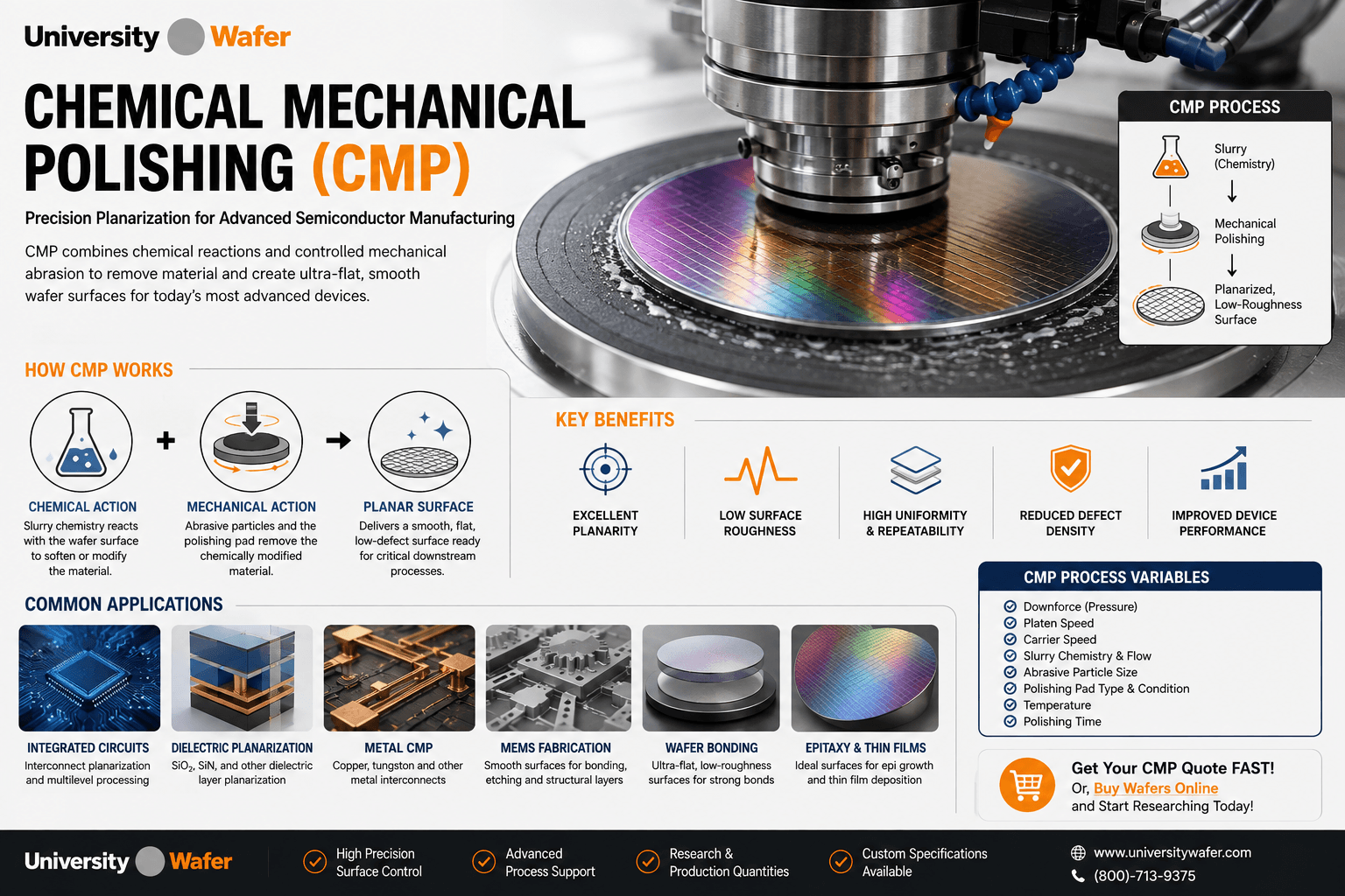
Chemical Mechanical Polishing (CMP), also called chemical mechanical planarization, is a precision surface-finishing process used to remove material and create highly planar semiconductor wafer surfaces. CMP combines controlled chemical reactions with mechanical polishing to achieve a surface quality that would be difficult to obtain using either method alone.
During CMP, a wafer is pressed against a rotating polishing pad while a specially formulated slurry is introduced between the wafer and pad. The slurry typically contains abrasive particles and chemical components that modify the wafer surface. The polishing action then removes the reacted material in a controlled manner.
This combination makes CMP an important process for silicon wafer polishing, semiconductor manufacturing, integrated circuits, MEMS, photonics, wafer bonding, and advanced materials research.
How Does CMP Work?
The Chemical Mechanical Polishing process relies on two mechanisms working together:
- Chemical action modifies or reacts with the material at the wafer surface.
- Mechanical action from the polishing pad and abrasive particles removes the chemically modified surface material.
The wafer is typically mounted in a carrier that controls pressure against the polishing pad. Both the carrier and polishing platen may rotate, creating controlled relative motion across the wafer surface.
Important CMP process variables can include downforce, platen speed, carrier speed, slurry chemistry, abrasive particle characteristics, slurry flow rate, polishing-pad properties, temperature, and polishing time.
CMP Slurry and Polishing Pads
The CMP slurry plays an important role in determining material removal rate, selectivity, surface quality, and defect formation. Different slurry chemistries can be developed for specific materials such as silicon, silicon dioxide, metals, and other semiconductor layers.
The polishing pad provides the mechanical interface between the wafer and polishing system. Pad hardness, surface texture, porosity, conditioning, and wear can all influence CMP performance.
Careful control of the slurry, pad, pressure, and polishing conditions helps researchers achieve the desired combination of surface smoothness, planarity, uniformity, and material removal rate.
Why Is Wafer Planarization Important?
Modern semiconductor devices contain multiple patterned and deposited layers. Each fabrication step can introduce topography across the wafer. Without planarization, these height variations can accumulate and interfere with subsequent processing.
CMP can reduce this topography and create a more uniform surface for additional fabrication steps. A planar wafer surface is particularly important for processes such as:
- Photolithography
- Thin-film deposition
- Epitaxial growth
- Wafer bonding
- Metallization
- Dielectric processing
- Multilevel integrated-circuit fabrication
CMP for Silicon Wafers
Silicon wafer CMP can be used during substrate preparation and semiconductor processing to achieve smooth, highly controlled surfaces. Polished silicon surfaces are important when subsequent fabrication steps depend on low surface roughness and good wafer planarity.
Researchers working with silicon wafers may require specific surface finishes depending on the intended application, including single-side polished (SSP) or double-side polished (DSP) substrates.
High-quality polished surfaces can be important for semiconductor processing, microscopy, thin-film research, optical applications, MEMS fabrication, and other experiments where surface condition can influence device performance or measurement accuracy.
Single-Side vs. Double-Side Polished Wafers
Wafer polishing requirements vary according to the intended application. Two common configurations are single-side polished (SSP) and double-side polished (DSP) wafers.
- Single-Side Polished (SSP): One wafer surface receives the primary polished finish while the opposite side may retain a different surface condition.
- Double-Side Polished (DSP): Both wafer surfaces are polished, making DSP substrates useful for applications requiring high-quality surfaces on both sides of the wafer.
Double-side polished wafers are often selected for applications involving wafer bonding, MEMS, optics, photonics, through-wafer processing, and precision metrology.
Surface Roughness and CMP
One of the primary objectives of CMP is to produce a controlled, low-roughness surface while maintaining the required wafer geometry. Surface roughness can affect thin-film growth, bonding quality, optical behavior, interface properties, and device fabrication.
Surface quality can be characterized using techniques such as Atomic Force Microscopy (AFM), profilometry, optical interferometry, and other surface metrology methods.
For demanding research applications, specifying the required surface roughness and measurement method can help ensure that the wafer is appropriate for the intended experiment.
CMP Applications in Semiconductor Research
Chemical Mechanical Polishing is used throughout semiconductor manufacturing and materials research. Common applications include:
- Silicon wafer surface preparation
- Integrated circuit planarization
- Oxide and dielectric planarization
- Metal interconnect processing
- MEMS fabrication
- Photonics research
- Wafer bonding preparation
- Thin-film research
- Epitaxial substrate preparation
- Advanced semiconductor packaging
Because CMP can influence both surface topography and surface condition, process parameters should be selected according to the substrate material, film being polished, and requirements of subsequent fabrication steps.
Choosing CMP Wafer Specifications
When requesting wafers or polishing services for research, useful specifications can include:
- Wafer material
- Wafer diameter
- Wafer thickness
- Crystal orientation
- Single-side or double-side polishing
- Target surface roughness
- Thickness and flatness requirements
- Film or material being polished
- Quantity required
Providing detailed specifications helps identify an appropriate substrate and surface finish for your semiconductor fabrication or materials research.
Get Your Chemical Mechanical Polishing (CMP) Quote FAST! Or, Buy Wafers Online and Start Researching Today!
CMP Materials and Surfaces
Chemical Mechanical Polishing (CMP) can be adapted to a variety of semiconductor materials, dielectric films, and conductive layers. The slurry chemistry, abrasive material, polishing pad, pressure, and process conditions are selected according to the material being removed and the desired final surface.
Materials commonly associated with CMP and wafer planarization include:
- Silicon (Si)
- Silicon dioxide (SiO2)
- Silicon nitride (Si3N4)
- Copper and other interconnect metals
- Tungsten
- Dielectric thin films
- Compound semiconductor materials
The optimum polishing process depends strongly on material properties and the required surface finish. CMP conditions developed for silicon, for example, should not automatically be assumed to work for a metal or compound semiconductor surface.
Oxide CMP and Dielectric Planarization
Oxide CMP is widely used to planarize silicon dioxide and related dielectric layers during semiconductor fabrication. As deposited and patterned layers accumulate, significant surface topography can develop across a wafer.
Controlled CMP can remove elevated regions and produce a flatter dielectric surface for subsequent lithography, deposition, metallization, or device processing.
This capability is particularly important in multilevel semiconductor structures where maintaining planarity becomes increasingly difficult as additional layers are fabricated.
Metal CMP for Semiconductor Interconnects
CMP is also an important process for metal interconnect fabrication. Conductive materials deposited into patterned structures can be selectively removed from elevated areas while remaining within trenches or vias.
Copper CMP is closely associated with damascene and dual-damascene semiconductor processing, where excess copper is removed after deposition to leave conductive interconnect structures within the dielectric.
Metal CMP requires careful control of removal rate and selectivity because excessive polishing can produce defects such as dishing, erosion, scratches, or nonuniform material removal.
CMP for Wafer Bonding
Surface condition is especially important for wafer bonding. Particles, excessive roughness, surface defects, or poor planarity can prevent intimate contact between two wafer surfaces and reduce bonding quality.
CMP may therefore be used as part of the preparation process for research involving:
- Direct wafer bonding
- Silicon-on-Insulator (SOI) structures
- Heterogeneous integration
- MEMS wafer bonding
- 3D semiconductor integration
- Advanced packaging
- Bonded semiconductor substrates
Researchers requiring bonded structures should consider surface roughness, flatness, cleanliness, bow, warp, and other wafer characteristics in addition to the polishing method itself.
CMP for MEMS Fabrication
MEMS fabrication often requires precise control of wafer thickness, surface topography, and deposited films. CMP can provide planar surfaces that support subsequent lithography, bonding, deposition, and micromachining steps.
Both silicon wafers and Silicon-on-Insulator (SOI) wafers are commonly used as starting substrates for MEMS research where wafer geometry and surface condition can influence fabrication results.
CMP and Epitaxial Growth
Epitaxial processes generally require carefully prepared substrate surfaces. Surface contamination, polishing damage, scratches, or excessive roughness can influence nucleation and subsequent crystal growth.
CMP can be part of the preparation sequence used to produce epi-ready wafer surfaces. Depending on the material system, additional cleaning and surface preparation may be required before epitaxial deposition.
Researchers planning epitaxial growth should specify the required surface finish rather than assuming that all polished wafers are automatically suitable for a particular epitaxy process.
Common CMP Defects
Although CMP is capable of producing extremely smooth and planar surfaces, improper process conditions can introduce defects. Understanding these defects is important when developing or evaluating a polishing process.
- Scratches: Surface damage caused by abrasive particles, contamination, or polishing conditions.
- Dishing: Excessive removal of softer material within recessed features.
- Erosion: Localized loss of material across patterned regions.
- Nonuniform removal: Differences in material removal across the wafer.
- Residual particles: Slurry or polishing contaminants remaining after CMP.
- Surface contamination: Chemical residues that may interfere with later processing.
Post-CMP cleaning is therefore an important part of many semiconductor processes because residual particles and chemicals can affect subsequent fabrication steps.
CMP Process Control
Successful Chemical Mechanical Polishing requires balancing material removal rate with surface quality and uniformity. Increasing polishing pressure or abrasive action may increase removal rate, but aggressive conditions can also increase the risk of surface damage.
Process development may involve monitoring:
- Material removal rate
- Within-wafer uniformity
- Wafer-to-wafer repeatability
- Surface roughness
- Film thickness
- Defect density
- Planarity
- Slurry condition
- Polishing pad condition
Measuring a CMP-Polished Surface
Several metrology techniques can be used to evaluate wafers after CMP. Atomic Force Microscopy (AFM) can characterize nanoscale surface topography and roughness, while profilometry can measure surface features, step heights, and related dimensional characteristics.
Optical techniques may also be used to evaluate wafer surfaces without physical contact. The appropriate measurement method depends on the material, expected roughness range, feature size, and research objective.
CMP for Research and Semiconductor Development
Chemical Mechanical Polishing supports many stages of modern semiconductor and materials research. From preparing smooth starting substrates to planarizing complex multilayer structures, CMP gives researchers a way to control surfaces before critical fabrication steps.
UniversityWafer supplies wafers and substrates for semiconductor fabrication, MEMS, photonics, thin-film deposition, wafer bonding, epitaxy, and materials research. When requesting polished substrates or related processing, provide the wafer material, diameter, thickness, surface finish, polishing requirements, target roughness, and quantity whenever possible.
Related Wafer Polishing & Processing Resources
- Silicon Wafers – Explore silicon substrates for semiconductor fabrication, MEMS, thin films, photonics, and materials research.
- Chemical Mechanical Polishing – Learn more about CMP processes used to produce smooth and planar semiconductor wafer surfaces.
- Atomic Force Microscopy (AFM) on Silicon Wafers – Learn how AFM is used to characterize nanoscale wafer surface roughness and topography.
- Profilometer Measurements & Thin-Film Stress – Explore profilometry, wafer curvature, surface measurements, and thin-film stress characterization.
- Low Surface Roughness Silicon Wafers – Learn about silicon wafer surface roughness requirements for precision semiconductor and materials research.
- Silicon-on-Insulator (SOI) Wafers – Explore SOI substrates used for MEMS, photonics, CMOS, sensors, and advanced semiconductor devices.
- Epi-Ready Semiconductor Wafers – Learn about surface preparation and wafer quality requirements for epitaxial growth.