
What Are Custom Sapphire Wafers?
Custom sapphire wafers are single-crystal aluminum oxide (Al2O3) substrates manufactured or selected to meet specific dimensional, crystallographic, and surface requirements. Sapphire has a corundum crystal structure and is an electrical insulator rather than a semiconductor.
Its combination of high hardness, chemical stability, electrical insulation, thermal stability, and optical transparency over a broad wavelength range makes sapphire useful as a substrate and optical material in research and device fabrication.
Researchers can explore our sapphire wafers and Al2O3 substrates for additional substrate options and specifications.
Custom Sapphire Crystal Orientations
Crystal orientation is one of the most important specifications when selecting a sapphire substrate. Because sapphire is crystallographically anisotropic, properties such as surface atomic arrangement, optical behavior, and the relationship between a substrate and an epitaxial film depend on orientation.
Common sapphire orientations include C-plane (0001), A-plane (11-20), R-plane (1-102), and M-plane (10-10). The appropriate orientation depends on the material being deposited and the requirements of the device or experiment.
C-plane sapphire is widely used for III-nitride epitaxy, including GaN-based structures. Other orientations can be useful when a different crystallographic relationship, surface symmetry, optical response, or growth behavior is required.
Sapphire Wafers for GaN Epitaxy
Sapphire is widely used as a substrate for gallium nitride on sapphire (GaN-on-sapphire) structures. GaN and related III-nitride materials are important for LEDs, laser diodes, RF electronics, power devices, and other optoelectronic technologies.
GaN is not lattice-matched to sapphire, so GaN-on-sapphire heteroepitaxy involves substantial lattice and thermal-expansion mismatch. Appropriate nucleation or buffer layers and carefully controlled epitaxial processes are therefore commonly used to manage nucleation and crystal quality.
Sapphire remains an important GaN substrate because it combines thermal stability, electrical insulation, availability, and compatibility with established III-nitride growth processes.
Custom Sapphire Wafer Dimensions
Custom sapphire substrates can be specified according to dimensional requirements such as diameter, thickness, shape, and dimensional tolerances. The appropriate dimensions depend on processing equipment, mechanical requirements, device layout, and the intended experiment.
Wafer thickness influences mechanical rigidity and handling, while geometric parameters such as total thickness variation (TTV), bow, and warp can become important for processes requiring precise wafer positioning, lithography, bonding, or uniform thin-film processing.
Researchers working with standard-size substrates can also explore 4-inch sapphire wafers for semiconductor, optical, and thin-film applications.
Single-Side and Double-Side Polished Sapphire
Sapphire wafers can be supplied with different surface finishes depending on the application. Single-side polished (SSP) sapphire provides one polished process surface, while double-side polished (DSP) sapphire provides polished surfaces on both sides.
DSP substrates can be useful for applications involving optical transmission, backside processing, bonding, or experiments requiring high-quality surfaces on both sides. SSP wafers may be sufficient when processing is performed primarily on one surface.
A polished appearance alone does not establish that a substrate is suitable for epitaxy. Applications involving epitaxial growth may require additional control of surface roughness, subsurface polishing damage, contamination, particles, and crystallographic orientation.
Sapphire Surface Quality and Roughness
Surface quality can directly influence thin-film deposition, epitaxial nucleation, bonding, optical performance, and nanoscale measurements. Scratches, particles, residues, pits, and excessive surface roughness can interfere with subsequent fabrication.
Surface topography can be characterized using techniques such as atomic force microscopy (AFM) . AFM can measure nanoscale surface-height variations over a defined scan area and is commonly used to quantify parameters such as root-mean-square (RMS) roughness.
Roughness values should always be interpreted together with the measurement method, scan size, filtering conditions, and required application rather than treated as a universal indicator of substrate quality.
Optical Properties of Sapphire
Single-crystal sapphire is transparent across a broad spectral range extending from portions of the ultraviolet through the visible and into the infrared, although the exact usable transmission range depends on crystal quality, thickness, surface finish, impurities, wavelength, and optical configuration.
Sapphire is also optically anisotropic and birefringent. Its refractive index depends on polarization and crystallographic direction, which should be considered in optical applications where polarization, orientation, or precise optical performance matters.
These characteristics make polished sapphire useful for selected optical windows, sensor components, optical experiments, and photonic research.
Mechanical and Chemical Properties
Sapphire is valued for its high hardness and resistance to mechanical wear. These properties can make it useful in environments where softer substrate materials may be more susceptible to scratching or abrasion.
Sapphire is also chemically stable against many environments, although it should not be described as chemically inert under all conditions. Its response to acids, bases, plasmas, and high-temperature processing depends on the chemistry and process conditions involved.
Choosing a Custom Sapphire Substrate
The best sapphire wafer specification depends on the complete fabrication or experimental process. Important parameters can include:
- Crystal orientation: C-plane, A-plane, R-plane, M-plane, or another specified cut.
- Diameter and shape: selected for equipment and experimental compatibility.
- Thickness: chosen according to mechanical, optical, and processing requirements.
- Surface finish: SSP, DSP, or an application-specific polished surface.
- Surface roughness: specified when thin-film growth, bonding, optics, or nanoscale surface quality is important.
- TTV, bow and warp: considered when wafer geometry affects processing or measurement.
- Orientation tolerance or miscut: specified when the crystallographic surface direction is important to epitaxy or other orientation-sensitive processes.
Custom Sapphire for Research and Fabrication
Customizing the substrate allows researchers to match the physical, crystallographic, optical, and surface properties of sapphire to the requirements of their experiment. Sapphire substrates can support applications involving III-nitride epitaxy, LEDs, RF devices, optical components, sensors, MEMS, thin-film deposition, and materials research.
For projects involving other crystalline substrate materials, explore our III-V semiconductor substrates and other wafer materials for advanced research and device development.
Get Your Custom Sapphire Wafer Quote FAST!
Or,
Buy Wafers Online
and Start Researching Today!
Custom Sapphire Wafers for Advanced Applications
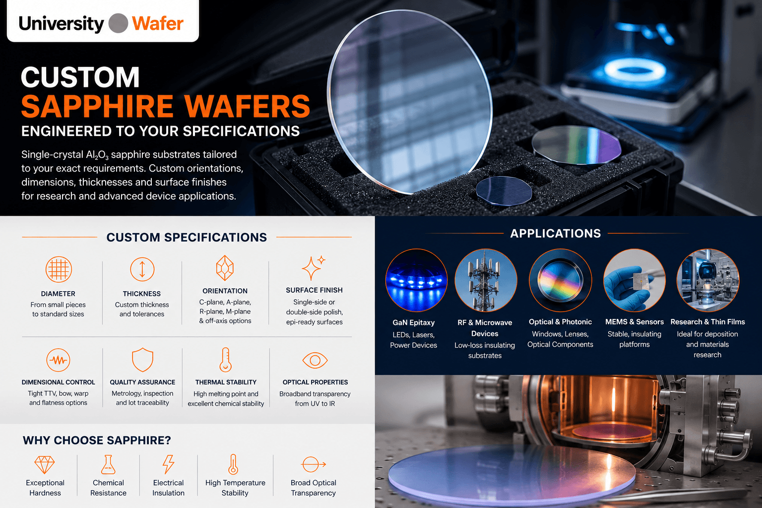
Custom sapphire wafers can be tailored to applications where crystallographic orientation, surface condition, dimensional tolerances, optical behavior, or electrical insulation are important. Because sapphire (Al2O3) is a single-crystal electrical insulator with high hardness and good thermal and chemical stability, it is used as a substrate in semiconductor, optical, RF, MEMS, and materials-research applications.
The appropriate substrate specification depends on the complete process. Orientation, thickness, polish, miscut, surface roughness, TTV, bow, and warp should therefore be selected according to the intended fabrication or characterization technique rather than treated as universal quality requirements.
Sapphire Substrates for GaN and III-Nitride Growth
One of the most important applications of sapphire is as a substrate for GaN-on-sapphire epitaxy . C-plane (0001) sapphire is widely used for the growth of GaN and related III-nitride heterostructures used in LEDs, laser diodes, RF electronics, and other semiconductor devices.
Sapphire and GaN have different crystal structures and substantial lattice mismatch, so high-quality GaN is not obtained simply by depositing GaN directly onto an untreated sapphire surface under arbitrary conditions. Practical epitaxial processes commonly employ nucleation layers, buffer layers, surface preparation, and optimized growth conditions to manage nucleation and reduce the effects of heteroepitaxial mismatch.
GaN structures can be grown using techniques such as metal-organic chemical vapor deposition (MOCVD) and molecular beam epitaxy (MBE) . Substrate requirements can differ according to the growth technique and epitaxial structure.
Sapphire for LEDs and Optoelectronics
Sapphire has played an important role as a substrate for III-nitride LEDs and laser structures. Its optical transparency and electrical insulation are useful characteristics for many GaN-based optoelectronic structures.
In these devices, sapphire primarily acts as the supporting substrate; the light-emitting semiconductor layers are III-nitride materials such as GaN, InGaN, or AlGaN. Sapphire itself is not the active semiconductor responsible for carrier injection and light emission.
Researchers investigating nitride materials can also explore AlGaN semiconductor materials for wide-bandgap heterostructures and optoelectronic research.
Sapphire Substrates for RF Devices
Sapphire's high electrical resistivity makes it useful as an electrically insulating substrate for selected RF and microwave structures. An insulating substrate can help reduce unwanted conductive paths through the substrate, although total RF loss also depends on dielectric properties, device geometry, metallization, frequency, interfaces, and the complete material stack.
Sapphire has also been used in silicon-on-sapphire and III-nitride device technologies. In silicon-on-sapphire (SOS) , a crystalline silicon layer is formed on a sapphire substrate, combining semiconductor functionality with an electrically insulating base.
Sapphire for Optical Components
Polished sapphire is used for selected optical components because it combines broad optical transmission with high hardness and mechanical durability. Applications can include optical windows, protective optical surfaces, sensor windows, spectroscopy components, and experimental optical substrates.
Sapphire is a uniaxial birefringent crystal, meaning its optical response depends on crystallographic direction and polarization. Orientation therefore matters when sapphire is used in optical systems where polarization or precise refractive behavior is important.
Surface polish, parallelism, thickness, orientation, and surface quality may all influence optical performance. Custom specifications can be particularly valuable when the substrate must satisfy both mechanical and optical requirements.
Custom Sapphire for Thin-Film Deposition
Sapphire provides a stable substrate for many thin-film deposition experiments. Depending on the material system, films can be deposited using techniques such as physical vapor deposition, chemical vapor deposition, atomic layer deposition, sputtering, evaporation, MOCVD, or MBE.
The resulting film quality depends on more than the sapphire itself. Surface preparation, crystal orientation, substrate temperature, deposition chemistry, lattice relationship, thermal-expansion mismatch, film thickness, and residual stress can all affect the deposited layer.
Researchers studying deposited films can use thin-film stress measurements to investigate substrate curvature and film-induced stress when the assumptions of the selected stress model are appropriate.
Sapphire Wafers for MEMS and Sensors
Custom sapphire can also be useful for selected MEMS, sensor, microfluidic, and harsh-environment research. Its electrical insulation, mechanical hardness, optical transparency, and stability at elevated temperatures can provide useful properties when silicon or glass does not meet a particular experimental requirement.
Sapphire is significantly harder to machine and etch than many common semiconductor and glass substrates. Fabrication processes must therefore be selected specifically for Al2O3 rather than assuming that conventional silicon etching or machining conditions will transfer directly to sapphire.
Miscut and Off-Axis Sapphire Wafers
In addition to nominal crystal orientation, a custom sapphire wafer may be specified with a controlled miscut or off-axis angle. A miscut describes a deliberate angular deviation of the polished surface from a specified crystallographic plane.
Controlled miscut can modify the surface step structure and can influence nucleation and step-flow behavior during certain epitaxial growth processes. The optimum angle and direction are specific to the material system and growth conditions, so an off-axis substrate should be selected according to the requirements of the intended epitaxial process.
Thermal Considerations for Sapphire Substrates
Sapphire remains mechanically and chemically stable over a broad range of processing conditions and can tolerate temperatures used in many semiconductor and thin-film processes. However, its thermal behavior should be evaluated as part of the complete device or film stack.
Sapphire's thermal conductivity is substantially lower than that of materials such as silicon carbide at room temperature. This can be important in high-power devices where heat removal through the substrate is a major design requirement.
Thermal-expansion mismatch between sapphire and a deposited film can also generate stress as the structure is heated or cooled. This is particularly relevant to heteroepitaxial films and thick deposited layers.
Characterizing Custom Sapphire Wafers
Different characterization techniques can be used to evaluate sapphire substrates depending on the property of interest. No single measurement provides a complete description of wafer quality.
- Atomic force microscopy (AFM): evaluates nanoscale surface topography and roughness over a specified scan area.
- X-ray diffraction (XRD): can be used to determine or verify crystallographic orientation and investigate structural characteristics.
- Optical inspection: can identify many visible scratches, particles, chips, and other surface or edge features.
- Interferometric measurements: can characterize surface figure, flatness, and other geometric or optical parameters depending on the instrument configuration.
- Optical spectroscopy: can evaluate wavelength-dependent transmission or other optical properties when required.
For nanoscale surface characterization, learn more about AFM surface characterization and its use in wafer and thin-film research.
How to Specify a Custom Sapphire Wafer
Providing a complete specification helps identify a sapphire substrate appropriate for the intended process. When requesting a custom Al2O3 wafer, consider specifying:
- Crystal orientation and orientation tolerance
- Miscut angle and direction, if required
- Diameter or custom substrate dimensions
- Wafer thickness and thickness tolerance
- Single-side or double-side polish
- Surface roughness requirements
- TTV, bow, warp, or flatness requirements
- Edge geometry or custom shape, when applicable
- Optical or surface-quality requirements
- Intended application or subsequent process
Clearly identifying which parameters are critical allows the substrate specification to be matched to the actual experiment rather than applying unnecessarily tight tolerances to every characteristic.
Custom Sapphire vs. Other Substrate Materials
Sapphire should be selected when its particular combination of properties benefits the application. It is not universally superior to silicon, glass, SiC, or other substrate materials. For example, silicon carbide wafers offer much higher thermal conductivity and are themselves wide-bandgap semiconductors, while sapphire provides electrical insulation, optical transparency, high hardness, and an established platform for III-nitride growth.
Similarly, glass wafers can provide optical transparency and electrical insulation at different cost, processing, and thermal-performance points. Substrate selection should therefore be based on the electrical, optical, thermal, mechanical, crystallographic, and fabrication requirements of the project.
Related Sapphire Wafer & Substrate Resources
- Sapphire Wafers & Al2O3 Substrates – Explore single-crystal sapphire substrates for semiconductor, optical, thin-film, and materials research.
- 4-Inch Sapphire Wafers – Explore 100 mm sapphire substrates for GaN epitaxy, optoelectronics, thin-film deposition, and research applications.
- GaN on Sapphire Wafers – Learn about gallium nitride layers grown on sapphire substrates for LEDs, optoelectronics, RF electronics, and III-nitride research.
- Silicon-on-Sapphire (SOS) Wafers – Explore crystalline silicon layers on electrically insulating sapphire substrates for RF, electronics, and specialized device research.
- MOCVD for Semiconductor Epitaxy – Learn how metal-organic chemical vapor deposition is used to grow GaN and other compound semiconductor epitaxial structures.
- Molecular Beam Epitaxy (MBE) – Explore controlled crystalline thin-film growth for semiconductor heterostructures and advanced materials research.
- Aluminum Gallium Nitride (AlGaN) – Learn about wide-bandgap AlGaN alloys used in III-nitride heterostructures, UV optoelectronics, and electronic devices.
- Atomic Force Microscopy (AFM) – Learn how AFM can characterize nanoscale surface roughness and topography on polished wafers and deposited thin films.
- Thin-Film Stress & Wafer Curvature – Explore methods for evaluating film-induced wafer curvature and thin-film stress in coated substrates.
- Silicon Carbide (SiC) Wafers – Compare sapphire with wide-bandgap SiC substrates for power, RF, epitaxial, and high-temperature semiconductor applications.
- Glass Wafers & Substrates – Explore electrically insulating and optically transparent glass substrates for MEMS, microfluidics, optics, and research.
- III-V Semiconductor Materials – Explore compound semiconductor substrates and materials for photonics, RF electronics, optoelectronics, and advanced research.