
What Is a Semiconductor Diode?
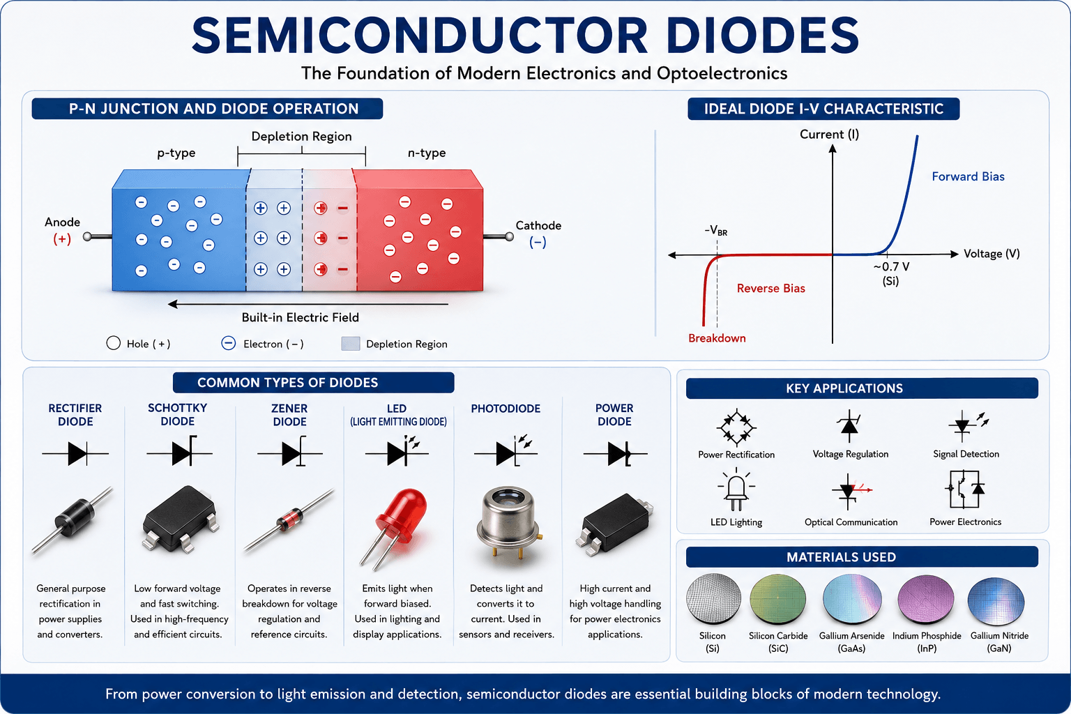
A semiconductor diode is a two-terminal electronic device designed to exhibit strongly asymmetric current-voltage behavior. Many common diodes are formed using a p-n junction, where p-type semiconductor and n-type semiconductor regions meet within a crystalline material.
Because of the electrical properties of this junction, a diode can conduct substantial current under suitable forward bias while allowing comparatively little current under reverse bias until breakdown mechanisms become important. This behavior makes diodes fundamental components in rectification, switching, voltage regulation, photodetection, light emission, and power electronics.
How Does a P-N Junction Work?
A p-n junction is created by adjoining semiconductor regions with different doping characteristics. The p-type region contains holes as its majority carriers, while the n-type region contains electrons as its majority carriers.
After the junction forms, electrons and holes initially diffuse across the interface because of the carrier concentration gradients. Electrons can recombine with holes near the junction, leaving behind ionized dopant atoms that are fixed in the crystal lattice.
This produces a region near the junction that is depleted of mobile majority carriers and contains net fixed charge. This region is known as the depletion region. The fixed charges create an internal electric field and electrostatic potential that oppose further majority-carrier diffusion. At thermal equilibrium, drift and diffusion currents balance so there is no net current through an unbiased ideal junction.
Forward Bias in a Semiconductor Diode
A p-n diode is forward biased when an external voltage is applied with the p-side at a higher electrical potential than the n-side. Forward bias reduces the junction's electrostatic barrier and narrows the depletion region, increasing carrier injection across the junction.
The current of an ideal p-n diode increases approximately exponentially with applied forward voltage over an appropriate operating range. Real devices deviate from ideal behavior because of effects including series resistance, recombination, high-level injection, temperature, and contact resistance.
Silicon p-n diodes are often described as having a forward voltage of roughly 0.6–0.7 V at typical operating currents, but this should not be treated as a fixed turn-on voltage. The actual forward voltage depends on current density, device structure, temperature, doping, area, and other parameters.
Reverse Bias and Diode Breakdown
Under reverse bias, the p-side is at a lower potential than the n-side. The applied voltage generally increases the junction barrier and widens the depletion region. Only a relatively small reverse current flows before breakdown in a conventional rectifying p-n diode.
If the reverse voltage becomes sufficiently large, the electric field can cause breakdown. Depending on junction design, doping, and electric-field distribution, breakdown can involve Zener tunneling, avalanche multiplication, or contributions from both mechanisms.
Breakdown is intentionally used in devices such as Zener and avalanche diodes for voltage-reference, regulation, and protection applications. In ordinary diodes not designed for sustained breakdown operation, excessive reverse current can damage the device.
Semiconductor Doping and Diode Fabrication
Semiconductor doping controls the concentrations of electrons and holes within a material. In silicon, acceptor impurities such as boron are commonly used to form p-type silicon, while donor impurities such as phosphorus or arsenic can be used to form n-type silicon.
Doping concentration influences important p-n junction characteristics, including depletion width, electric-field distribution, junction capacitance, series resistance, and breakdown behavior. Semiconductor device fabrication can use techniques such as ion implantation, diffusion, and doped epitaxial growth to establish the required doping profiles.
Researchers studying diode fabrication can select semiconductor wafers with specified conductivity type, resistivity, orientation, thickness, and surface finish according to the requirements of the experiment or device.
Silicon Diodes
Silicon wafers are widely used for diode fabrication because silicon processing is mature, high-quality thermal SiO2 can be formed on silicon, and a broad manufacturing infrastructure exists for silicon semiconductor devices.
Silicon diode technologies include small-signal diodes, rectifiers, photodiodes, avalanche devices, Zener diodes, and many power-device structures. The appropriate wafer specifications depend on factors such as voltage rating, current density, junction depth, device geometry, and fabrication process.
Wide-Band-Gap Semiconductor Diodes
Wide-band-gap semiconductor materials are particularly important for high-power, high-voltage, and high-temperature device research. Silicon carbide (SiC) has a substantially higher critical electric field than silicon and is widely used in power-electronic devices, including commercial SiC Schottky barrier diodes.
Gallium nitride is another important wide-band-gap semiconductor. GaN-based structures are studied and manufactured for power electronics, RF electronics, and optoelectronic devices. Researchers can explore GaN-on-sapphire substrates and other GaN material systems according to their epitaxial and device requirements.
Compound Semiconductors for Optoelectronic Diodes
Compound semiconductors are especially important when a diode must efficiently interact with light. Materials with direct band gaps can provide efficient radiative transitions, making III-V semiconductors important for light-emitting diodes (LEDs), laser diodes, and photodetectors.
Gallium arsenide (GaAs) and indium phosphide (InP) are examples of III-V semiconductor materials used as substrates or constituents of epitaxial device structures for optoelectronic and high-frequency applications.
Why Wafer Properties Matter for Diode Research
The starting substrate can influence both semiconductor processing and final device behavior. Important specifications can include semiconductor material, conductivity type, dopant species, resistivity, crystal orientation, thickness, surface quality, and defect density.
UniversityWafer supplies semiconductor wafers and substrates for diode research, semiconductor device fabrication, optoelectronics, power-device development, sensors, and university laboratories.
Get Your Semiconductor Wafer Quote FAST!
Or,
Buy Wafers Online
and Start Researching Today!
Common Types of Semiconductor Diodes
Semiconductor diodes can be engineered for very different electrical and optical functions. Although the p-n junction diode is one of the most familiar structures, not every diode relies on a conventional p-n junction. For example, a Schottky diode uses a metal-semiconductor junction, while specialized photodiodes and light-emitting diodes use structures optimized for interaction with light.
Material selection, doping profile, junction geometry, layer thickness, band structure, and device architecture determine characteristics such as forward voltage, reverse leakage, switching behavior, capacitance, breakdown voltage, optical response, and allowable current density.
Rectifier Diodes
Rectifier diodes are designed to conduct current primarily in one direction and block it in the opposite direction. They are widely used to convert alternating current (AC) into direct current (DC) in power supplies, battery chargers, converters, and other power-electronic systems.
Rectifier performance depends on parameters including forward voltage drop, reverse-voltage capability, leakage current, current rating, switching behavior, junction temperature, and thermal management. Different semiconductor materials and device structures are therefore selected according to the voltage, frequency, efficiency, and power requirements of the application.
Schottky Barrier Diodes
A Schottky diode is formed using a rectifying metal-semiconductor junction rather than a conventional p-n junction. In many applications, Schottky diodes provide relatively low forward voltage and fast switching because their operation can be dominated by majority-carrier transport.
Silicon Schottky diodes are widely used in lower-voltage rectification and high-frequency circuits. For higher-voltage power electronics, silicon carbide (SiC) is particularly important. SiC's wide band gap and high critical electric field enable Schottky barrier devices designed for substantially higher blocking voltages than are practical for many conventional silicon Schottky structures.
Zener and Avalanche Diodes
Zener diodes and avalanche diodes are designed to operate in controlled reverse breakdown. When the reverse voltage reaches the appropriate breakdown region, current can increase strongly while the voltage across the device remains within a comparatively narrow range over its specified operating conditions.
Reverse breakdown can involve quantum-mechanical tunneling, commonly associated with strongly doped junctions and relatively low breakdown voltages, or avalanche multiplication, in which carriers gain sufficient energy from the electric field to generate additional electron-hole pairs by impact ionization. Practical devices can exhibit contributions from both mechanisms.
These diodes are used for applications including voltage references, voltage regulation, transient suppression, and circuit protection.
Photodiodes and Optical Detection
A photodiode converts absorbed optical energy into an electrical response. Photons with sufficient energy can generate electron-hole pairs in the semiconductor, and an internal electric field can separate photogenerated carriers to produce photocurrent.
Photodiodes may operate under reverse bias or, in some applications, at or near zero external bias. Important performance parameters include responsivity, spectral response, dark current, junction capacitance, bandwidth, noise, and active area.
The semiconductor material strongly affects the wavelengths that can be detected. Silicon is widely used for visible and near-infrared detection, while compound semiconductors such as gallium arsenide (GaAs) and indium phosphide (InP) are important substrate and epitaxial-material platforms for specialized optoelectronic devices. InGaAs-based photodiodes, commonly grown on InP, are especially important for near-infrared optical communications.
PIN Photodiodes
A PIN diode contains p-type and n-type regions separated by a relatively lightly doped or nominally intrinsic region. Under reverse bias, much of this central region can become depleted, creating a broad electric-field region in which photogenerated carriers can be collected.
PIN structures are widely used in photodetectors because they can provide useful combinations of quantum efficiency, capacitance, response speed, and active-region thickness. PIN diode structures are also used in RF and microwave applications, where carrier storage in the central region can be exploited for switching and attenuation.
Avalanche Photodiodes
Avalanche photodiodes (APDs) operate at high reverse electric fields so that photogenerated carriers can trigger impact ionization. The resulting avalanche multiplication provides internal electrical gain before the signal reaches external readout electronics.
This gain can improve sensitivity in appropriate detection systems, but APDs generally require careful control of operating voltage, temperature, noise, and electric-field distribution. Material and epitaxial-layer design are therefore critical to APD performance.
Light-Emitting Diodes (LEDs)
A light-emitting diode (LED) converts electrical energy into light through radiative electron-hole recombination. Efficient LEDs generally use direct-band-gap semiconductor materials because direct transitions can produce photons efficiently without requiring a simultaneous change in crystal momentum through phonon participation.
III-V compound semiconductors are therefore central to LED technology. GaAs-based and related alloy systems are used for infrared and visible optoelectronics, while GaN and its alloys are fundamental to blue, violet, and many white-light LED technologies.
Researchers working with III-V materials can explore GaAs substrates and GaN-on-sapphire substrates for compound-semiconductor and optoelectronic research.
Laser Diodes
Laser diodes are electrically driven semiconductor devices in which injected electrons and holes can recombine within an active region to produce stimulated emission. Optical confinement and feedback are incorporated into the device so that coherent light can be generated above the lasing threshold.
Semiconductor lasers commonly use compound-semiconductor heterostructures and quantum wells rather than a simple homojunction. Material composition and layer design determine properties including emission wavelength, carrier confinement, optical confinement, threshold behavior, and efficiency.
Power Diodes and Wide-Band-Gap Materials
Power diodes are designed to handle higher currents, voltages, or power levels than small-signal devices. Their structures must balance forward conduction losses with reverse blocking capability and switching performance.
Wide-band-gap materials such as silicon carbide are especially important for modern power electronics. Compared with silicon, SiC has a wider band gap and substantially higher critical electric field, allowing device designs that can support high blocking voltages while using relatively thin, more heavily doped drift regions.
These properties make SiC diode technology important for electric vehicles, renewable-energy converters, industrial power supplies, charging systems, motor drives, and other high-efficiency power-conversion applications.
Diode I-V Characteristics
The current-voltage (I-V) characteristic is one of the fundamental measurements used to evaluate a diode. It shows how device current changes as the applied voltage moves through forward bias, reverse bias, and, where appropriate, reverse breakdown.
For an ideal p-n junction, the current-voltage relationship is commonly described using the Shockley diode equation:
I = IS[exp(qV/nkT) - 1]
where I is diode current, IS is the reverse saturation-current parameter, q is the elementary charge, V is the junction voltage, n is the ideality factor, k is Boltzmann's constant, and T is absolute temperature. Real devices can depart substantially from this idealized relationship due to series resistance, recombination, leakage mechanisms, high-level injection, and other physical effects.
Temperature Effects on Diodes
Diode performance is temperature dependent. Temperature influences intrinsic carrier concentration, recombination and generation, carrier transport, leakage current, forward voltage, and breakdown behavior. The exact temperature dependence varies with semiconductor material and device structure.
Thermal management is particularly important in power devices because electrical losses generate heat and device characteristics can change as junction temperature increases. Substrate material, die attachment, packaging, and cooling therefore contribute to overall device performance and reliability.
Semiconductor Materials for Diode Fabrication
There is no single best semiconductor material for every diode. Material selection depends on the required electrical and optical characteristics. Silicon wafers are widely used for rectifiers, Zener devices, photodiodes, and many conventional semiconductor components.
SiC wafers are important for high-voltage and high-power diode technologies, while GaAs , InP , GaN, and related compound-semiconductor systems enable specialized optoelectronic, RF, and high-performance device structures.
Diode Research and Device Fabrication
Experimental diode fabrication can involve semiconductor device manufacturing processes such as wafer cleaning, oxidation, epitaxial growth, thin-film deposition, photolithography, etching, doping, annealing, metallization, passivation, and electrical characterization.
Starting-wafer specifications such as conductivity type, resistivity, crystal orientation, thickness, surface finish, and defect quality should be selected according to the diode architecture and fabrication process. UniversityWafer supplies semiconductor wafers and substrates for diode fabrication, power electronics, photonics, sensors, optoelectronics, and semiconductor research.
Related Semiconductor Diode Resources
- Semiconductor Wafers – Explore semiconductor substrates for diode fabrication, electronics, sensors, power devices, and optoelectronic research.
- Semiconductor Device Manufacturing – Learn about wafer processing, lithography, etching, doping, deposition, metallization, and other semiconductor fabrication processes.
- Silicon Wafers – Explore silicon substrates for p-n junction diodes, rectifiers, photodiodes, sensors, and semiconductor device research.
- P-Type Silicon – Learn how acceptor doping produces p-type silicon used in p-n junctions and semiconductor device structures.
- Silicon Doping and Carrier Mobility – Explore how semiconductor doping influences carrier concentration, mobility, resistivity, and device behavior.
- Silicon Carbide (SiC) Wafers – Explore wide-band-gap SiC substrates used in power-electronic research and high-voltage semiconductor devices.
- Gallium Arsenide (GaAs) Wafers – Learn about GaAs substrates for optoelectronic, RF, photodetector, LED, and compound-semiconductor research.
- Indium Phosphide (InP) Wafers – Explore InP substrates for photonics, laser diodes, photodetectors, and high-speed optoelectronic devices.
- Gallium Nitride on Sapphire – Explore GaN-on-sapphire structures for LED, optoelectronic, and wide-band-gap semiconductor research.
- Silicon Band Gap – Learn how silicon's electronic band structure relates to carrier generation, optical absorption, and semiconductor device behavior.
- Fermi Level in Semiconductors – Explore the semiconductor Fermi level and its relationship to doping, carrier populations, and electronic devices.
- Intrinsic Carrier Concentration – Learn how temperature and semiconductor band structure influence equilibrium electron and hole concentrations.