
Double Side Polished (DSP) Silicon Wafers
Double side polished (DSP) silicon wafers have polished surfaces on both the front and backside of the substrate. Unlike single-side polished (SSP) wafers, DSP wafers provide two smooth, controlled surfaces that can be used for lithography, bonding, optical access, backside processing, metrology, MEMS fabrication, and other processes requiring access to both sides of the wafer.
UniversityWafer supplies prime-grade silicon wafers and test-grade silicon wafers with double-side polished surfaces. Available specifications may include multiple wafer diameters, thicknesses, crystal orientations, conductivity types, dopants, resistivity ranges, and surface-quality requirements.
DSP wafers can also be supplied with tightly controlled total thickness variation (TTV), bow, warp, and surface roughness when required. These parameters should be specified independently because double-side polishing alone does not guarantee a particular TTV, bow, or warp value.
Why Polish Both Sides of a Silicon Wafer?
Silicon wafer polishing removes subsurface damage and produces a smooth surface suitable for precision fabrication and characterization. With a DSP wafer, both major surfaces receive polishing, allowing processes to use either side of the substrate.
This can be particularly useful when a process requires:
- Frontside and backside photolithography
- Wafer-to-wafer or wafer-to-glass bonding
- Backside alignment
- Optical access through or across the substrate
- MEMS structures processed from both sides
- Surface-sensitive thin-film deposition
- Precision thickness or surface metrology
- Controlled surfaces for thinning and subsequent processing
DSP should therefore be selected because the fabrication process requires two polished surfaces, rather than assuming that DSP is automatically superior to SSP for every application.
DSP Silicon Wafers for MEMS
MEMS fabrication is an important application for double side polished silicon, especially when structures must be patterned, etched, aligned, bonded, or inspected from both sides of the wafer.
Examples include microfluidic structures, membranes, cavities, cantilevers, pressure sensors, inertial sensors, resonators, and other micromachined devices. DSP wafers can also facilitate double-sided lithography and alignment when features on opposite surfaces must be registered accurately.
However, DSP is not required for every MEMS device. Single-side polished silicon may be sufficient when fabrication occurs primarily on one surface. The correct choice depends on the device architecture and process flow.
Low TTV, Bow and Warp DSP Silicon
Wafer geometry can be critical in precision fabrication. Important specifications include:
- Total Thickness Variation (TTV): the difference between the maximum and minimum wafer thickness measured under the specified measurement conditions.
- Bow: a measure of the displacement of the wafer's median surface relative to a reference plane when the wafer is measured in a specified free, unclamped condition.
- Warp: a measure related to the overall deviation of the wafer median surface from a reference plane, including more complex wafer-shape distortion.
- Surface Roughness (Ra): an arithmetic average measure of surface-height deviations over the specified measurement area and conditions.
Tight control of these parameters may be important for photolithography, bonding, MEMS, metrology, thin-film processing, and precision wafer handling.
UniversityWafer inventory may include DSP silicon with very tight TTV and surface specifications. When requesting a quote, specify the actual maximum TTV, bow, warp, and roughness required by your process rather than relying only on the DSP designation.
DSP Silicon for Wafer Bonding
Wafer bonding is another important use for double-side polished silicon. Bonding processes can be sensitive to surface roughness, particles, contamination, flatness, bow, and warp.
Depending on the process, DSP silicon may be used for direct bonding, anodic bonding to suitable glass substrates, adhesive bonding, or other wafer-level integration techniques. The required surface preparation and geometry depend on the specific bonding mechanism.
Double Side Polished Ultra-Thin Silicon Wafers
DSP processing can be useful for ultra-thin silicon wafers, particularly when both surfaces must have controlled roughness or when backside processing is required after thinning.
Very thin silicon becomes increasingly flexible and mechanically fragile as thickness decreases. Handling, grinding, lapping, polishing, temporary bonding, stress control, and edge condition can therefore become important parts of the thinning process.
Backside polishing does not by itself prevent a thin wafer from warping. Final wafer shape depends on factors including residual stress, thickness uniformity, surface processing, deposited films, thermal history, crystal properties, and handling conditions.
DSP vs. SSP Silicon Wafers
| Feature | DSP Silicon | SSP Silicon |
|---|---|---|
| Polished Surfaces | Front and backside | One primary polished surface |
| Backside Lithography | Well suited | Depends on backside condition and process |
| Double-Sided Processing | Well suited | Less commonly selected |
| Wafer Bonding | Useful when both polished surfaces are required | Suitable for processes requiring only one polished bonding surface |
| Optical / Backside Inspection | Can be advantageous | Backside finish may limit some measurements |
| Typical Cost | Generally higher due to additional processing | Generally lower |
How to Specify a DSP Silicon Wafer
To receive the most appropriate double side polished silicon wafer, provide as many of the following specifications as possible:
- Diameter
- Thickness and tolerance
- Crystal orientation — such as Si(100), Si(110), or Si(111)
- CZ or FZ crystal growth
- P-type, n-type, or high-resistivity material
- Dopant
- Resistivity (Ω·cm)
- Maximum TTV
- Bow and warp limits, when required
- Front and backside surface roughness
- Edge profile or edge exclusion requirements
- Quantity
- Intended application
Request Double Side Polished Silicon Wafers
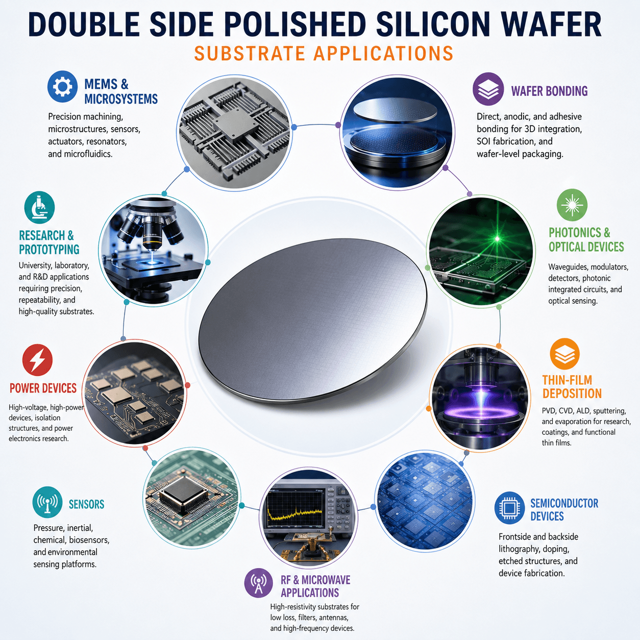
UniversityWafer supplies DSP silicon for semiconductor research, microfabrication, MEMS, wafer bonding, photonics, sensors, thin-film processing, and other applications requiring polished front and backside surfaces.
Get Your DSP Silicon Wafer Quote FAST! Or, Buy Wafers Online and start researching today!
Double Side Polished Silicon Wafer Inventory
UniversityWafer supplies double side polished (DSP) silicon wafers with a wide range of electrical, crystallographic, dimensional, and surface specifications. Available material may include Czochralski (CZ) and Float Zone (FZ) silicon, p-type and n-type material, high-resistivity silicon, multiple crystal orientations, and both standard and custom thicknesses.
The inventory below includes examples of DSP silicon with tightly controlled total thickness variation (TTV). Some configurations may also specify bow, warp, orientation tolerance, resistivity, wafer flats or notches, and other parameters important for precision fabrication.
Inventory and availability can change. When selecting a wafer, verify the complete specification rather than assuming that all DSP wafers have the same surface quality or dimensional tolerances.
Material - CZ unless noted |
|||||||
| Item | Type/Dop | Ori. | Dia(mm) | Thk(μm) | Polish | Res Ωcm | Notes |
| 6971 | n-type Si:P | [100--25° towards[110]] ±1° | 6" | 675 | DSP | 1--100 | SEMI notch Prime, Empak cst, TTV<1μm |
| S5594 | P/B | [100] | 5" | 990 ±8 | DSP | 1--25 | SEMI Prime, Empak cst, TTV<1μm |
| D868 | P/B | [100] | 5" | 590 | DSP | 1--30 | SEMI Prime with Notch, TTV<1μm, Bow/Warp<10μm, Empak cst |
| F709 | n-type Si:P | [100] | 5" | 762 ±12 | DSP | 5--35 | SEMI Prime, 1Flat, Empak cst, TTV<1μm, Bow<5μm, Warp<10μm |
| S6284 | n-type Si:P | [100] ±1° | 4" | 200 ±10 | DSP | FZ >1,000 | SEMI Prime, 1Flat, TTV<1μm, in Empak cst |
| G706 | Intrinsic Si:- | [100] | 4" | 500 | DSP | FZ >20,000 | SEMI Prime, 1Flat, TTV<1μm, Empak cst |
| 6356 | Intrinsic Si:- | [100] | 4" | 500 | DSP | FZ >20,000 | SEMI Prime, 1Flat, TTV<1μm, Empak cst |
| J302 | P/B | [100] | 4" | 600 | DSP | 1--50 | SEMI Prime, 1Flat, TTV<μm, Empak cst |
| 7089 | P/B | [100] | 4" | 381 ±7 | DSP | 0.014--0.021 | Prime, 2Flats, Empak cst, TTV<1μm |
| F022 | P/B | [111] ±0.3° | 4" | 350 ±5 | DSP | <0.05 | SEMI Prime, 1Flat, Empak cst, TTV<1μm, Bow/Wrp<15μm |
| 6570 | n-type Si:P | [100] | 4" | 400 | DSP | 1--10 | SEMI Prime, 2Flats, TTV<1μm, With lasermark, Empak cst |
| 4975 | n-type Si:Sb | [211] ±0.5° | 4" | 1,500 ±15 | DSP | 0.01--0.02 | SEMI Prime, 1Flat, Empak cst, TTV<1μm |
| S962 | Intrinsic Si:- | [100] | 4" | 525 | DSP | FZ >20,000 | SEMI Prime, 1Flat, Super Low TTV<0.3μm over entire wafer, Empak cst |
| D796 | P/B | [100] | 4" | 500 | DSP | 1--30 | SEMI Prime, 1Flat, Empak cst, TTV<1μm |
| L302 | P/B | [100] | 4" | 625 | DSP | 1--50 | SEMI Prime, 1Flat,TTV<1μm, Empak cst |
| Q787 | P/B | [111] ±0.5° | 4" | 350 | DSP | 0.001--0.005 | SEMI Prime, 1Flat, Empak cst, TTV<1μm |
| J066 | n-type Si:P | [100] | 4" | 500 | DSP | 1--100 | SEMI Prime, 2Flats, TTV<1μm, With Lasermark, Empak cst |
| 4154 | P/B | [110] ±0.5° | 3" | 360 | DSP | 1--10 | SEMI Prime, 2Flats, TTV<1μm, 1--2 weeks ARO o repolish |
| 6826 | P/B | [100] | 3" | 475 | DSP | 1--50 | SEMI Prime, 2Flats, Empak cst, TTV<0.3μm |
| D750 | P/B | [100] | 3" | 420 | DSP | <1 | SEMI Prime, 2Flats, Empak cst, TTV<1μm |
| S5580 | n-type Si:P | [100] ±1° | 3" | 2,286 ±13 | DSP | 15--28 | SEMI Prime, 1Flat, TTV<1μm, Sealed in individual csts, in groups of 5 wafers |
| S5824 | n-type Si:P | [100] ±1° | 3" | 300 ±10 | DSP | 5--15 | SEMI Prime, TTV<1μm, Empak cst |
| 6400 | n-type Si:P | [100] | 3" | 350 | DSP | 1--25 | SEMI Prime, 1Flat, TTV<1μm, Empak cst |
| 6818 | n-type Si:P | [100] | 3" | 381 | DSP | 1--30 | SEMI Prime, 2Flats, Empak cst, TTV<1μm |
| H988 | P/B | [100] | 3" | 580 | DSP | 1--100 | SEMI Prime, 1Flat, TTV<1μm, Lasermark, Empak cst |
Understanding the DSP Inventory Specifications
A DSP inventory table contains several specifications that should be considered together. The polishing designation describes the surface finish, while electrical, crystallographic, and geometric parameters determine whether the substrate is suitable for a particular experiment or fabrication process.
Type and Dopant
Silicon conductivity is controlled by electrically active dopants. Boron (B) is commonly used as an acceptor to produce p-type silicon, while phosphorus (P) and antimony (Sb) are donor dopants used to produce n-type silicon.
The conductivity type and dopant should be selected according to the electrical requirements of the device. They are independent of whether the wafer is SSP or DSP.
Crystal Orientation
The orientation identifies the crystallographic plane approximately parallel to the wafer surface. Common silicon wafer orientations include Si(100), Si(110), and Si(111), although specialty orientations and intentional off-axis cuts are also available.
Orientation can influence anisotropic etching, surface atomic structure, oxidation behavior, epitaxial growth, and other fabrication processes. Learn more about silicon wafer orientation.
Wafer Thickness
Wafer thickness affects mechanical stiffness, handling, device geometry, thermal behavior, and compatibility with fabrication equipment. DSP silicon is available in both conventional and specialty thicknesses.
For applications requiring substantially reduced substrate thickness, see ultra-thin silicon wafers.
Electrical Resistivity
Silicon resistivity is commonly specified in ohm-centimeters (Ω·cm) and is related to the concentration and mobility of charge carriers in the material.
Low-resistivity silicon contains a relatively high concentration of electrically active dopants and is useful when greater electrical conductivity is required. Higher-resistivity material has lower free-carrier concentration and can be advantageous for RF, microwave, detector, photonic, dielectric-isolation, and other specialized applications.
High-Resistivity FZ Double Side Polished Silicon
Float Zone (FZ) silicon is produced using a crucible-free crystal-growth process. Compared with conventional CZ silicon, FZ material generally contains substantially less oxygen and can be manufactured with very high electrical resistivity.
High-resistivity DSP FZ wafers can be useful for applications in which substrate conduction or RF loss must be minimized. Examples include microwave devices, RF structures, detectors, photonics, high-frequency characterization, and specialized sensor research.
High resistivity alone does not determine RF or photonic performance. Surface condition, interface states, oxide charge, device geometry, frequency, processing history, and other material properties can also influence substrate-related losses.
What Does Low TTV Mean?
Total Thickness Variation (TTV) describes the difference between the maximum and minimum measured thickness of a wafer under a defined measurement method and condition.
A lower TTV indicates more uniform thickness across the wafer. Tight TTV can be particularly important for precision lithography, wafer bonding, MEMS, thinning, optical processing, and applications where thickness uniformity affects the final device geometry.
Some DSP wafers can be manufactured with exceptionally tight TTV, but DSP and low TTV are not synonymous. TTV must be specified and measured independently from surface polish.
TTV, Bow and Warp Are Different Specifications
TTV, bow, and warp describe different aspects of wafer geometry and should not be used interchangeably.
- TTV describes variation in wafer thickness.
- Bow describes a global curvature-related displacement of the wafer median surface relative to a reference plane under defined measurement conditions.
- Warp describes overall deviation of the wafer median surface from a reference plane and can capture more complex wafer-shape distortion.
A wafer can therefore have very low TTV while still exhibiting measurable bow or warp. When wafer geometry is critical, specify acceptable limits for each relevant parameter.
DSP Silicon for Backside Lithography
Double-side polishing is particularly useful when both sides of the wafer participate in the fabrication process. A polished backside can facilitate backside photoresist processing, alignment, inspection, metrology, and pattern transfer.
Double-sided processing is common in selected MEMS and sensor fabrication processes where frontside structures must be aligned with backside cavities, membranes, vias, or other features.
Actual alignment accuracy is determined by the lithography equipment, alignment marks, wafer geometry, optical properties, process design, and other factors; DSP alone does not establish alignment accuracy.
DSP Silicon for Wafer Bonding
Wafer bonding can benefit from DSP substrates when the process requires controlled surfaces on both sides of the silicon wafer.
Bonding quality may depend on surface roughness, particles, contamination, flatness, bow, warp, surface chemistry, and bonding conditions. These requirements can be particularly demanding for direct wafer bonding, where intimate contact between very smooth and clean surfaces is important.
Other bonding methods, including anodic, adhesive, eutectic, and intermediate-layer bonding, have different surface and process requirements.
DSP Silicon for MEMS and Sensors
Double side polished silicon is commonly selected for MEMS and sensor processes that require fabrication from both wafer surfaces. Applications may include:
- Pressure-sensor diaphragms
- Micromachined membranes
- Accelerometers and inertial structures
- Microfluidic devices
- Resonators
- Backside cavities
- Through-wafer structures
- Wafer-level sensor packaging
Silicon is particularly useful for MEMS because its mechanical properties, crystal structure, processing chemistry, and compatibility with established semiconductor fabrication methods are well characterized.
DSP Silicon for Photonics and Optical Research
DSP silicon can also be useful in photonic and optical experiments when both substrate surfaces must have controlled finishes or when backside processing, bonding, thinning, or optical characterization is required.
Crystalline silicon is not transparent throughout the visible spectrum, but it becomes useful as an optical material over portions of the near-infrared and infrared spectrum where absorption is sufficiently low for the intended application. Exact transmission depends on wavelength, thickness, doping, temperature, and material quality.
For integrated photonic structures requiring a thin silicon device layer above an insulating layer, silicon-on-insulator (SOI) may be more appropriate than a conventional bulk DSP wafer.
DSP Silicon for Thin-Film Deposition
Double-side polished wafers provide controlled surfaces for thin-film deposition and materials research. Depending on the experiment, films may be deposited by sputtering, evaporation, chemical vapor deposition (CVD), atomic layer deposition (ALD), or other techniques.
Processing both sides can be useful for stress-compensation studies, backside coatings, optical structures, sensors, bonding layers, and other experimental architectures.
Film stress can also change wafer bow and warp after deposition, even when the starting DSP substrate has tightly controlled geometry.
CZ vs. FZ DSP Silicon Wafers
| Property | CZ Silicon | FZ Silicon |
|---|---|---|
| Growth Method | Crystal pulled from a silicon melt contained in a silica crucible | Localized molten zone passes through a silicon rod without a containing crucible |
| Oxygen Content | Generally higher due primarily to interaction with the silica crucible | Generally much lower |
| High-Resistivity Availability | Available, depending on specification and growth process | Especially well suited to very high-resistivity material |
| Large-Diameter Availability | Broad commercial availability | More limited than CZ, especially at larger diameters |
| Typical Research Uses | General semiconductor, MEMS, sensors and microfabrication | RF, detectors, photonics and high-resistivity applications |
Selecting the Right Double Side Polished Silicon Wafer
The correct DSP substrate depends on the complete fabrication process. Researchers should consider more than diameter and polish when comparing wafers.
Important parameters include:
- Diameter and thickness
- CZ or FZ crystal growth
- P-type or n-type conductivity
- Dopant species
- Electrical resistivity
- Crystal orientation and orientation tolerance
- Total Thickness Variation (TTV)
- Bow and warp
- Front and backside surface roughness
- Flat or notch configuration
- Edge condition
- Quantity and intended process
Providing the intended application—such as MEMS, wafer bonding, lithography, RF, photonics, deposition, or thinning—can help identify an appropriate wafer specification.
Double Side Polished Silicon Wafers for Research
UniversityWafer supplies DSP silicon substrates for universities, laboratories, semiconductor development, MEMS, photonics, sensors, wafer bonding, thin-film research, and other precision fabrication applications.