
Choosing GaAs Wafers for Photonics Research
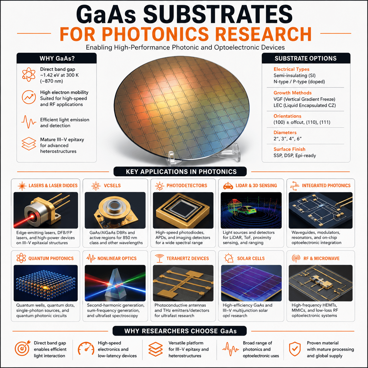
Gallium arsenide (GaAs) wafers are widely used as substrates for photonics, optoelectronics, high-frequency electronics, semiconductor epitaxy, and advanced device research. GaAs is a III-V compound semiconductor with a direct band gap of approximately 1.42 eV at room temperature, making GaAs-based material systems particularly important for light-emitting and light-detecting devices.
GaAs substrates support applications including laser diodes, LEDs, photodetectors, optical sensors, VCSELs, high-efficiency solar cells, integrated photonics, RF devices, and semiconductor heterostructures. In many photonic devices, the GaAs wafer acts as the crystalline substrate on which additional III-V semiconductor layers are grown epitaxially.
UniversityWafer supplies GaAs wafers in semi-insulating and conductive configurations, with multiple orientations, diameters, thicknesses, surface finishes, and crystal-growth options for research and device fabrication.
Why GaAs Is Important for Photonics
One of the most important differences between GaAs and silicon is their electronic band structure. GaAs has a direct fundamental band gap, whereas crystalline silicon has an indirect band gap.
In a direct-band-gap semiconductor, electrons near the conduction-band minimum can recombine radiatively with holes near the valence-band maximum without requiring a phonon to provide a large change in crystal momentum. This makes direct-gap III-V material systems particularly effective for light emission.
GaAs also has high electron mobility relative to silicon under comparable low-field conditions, which contributes to its importance in high-frequency and high-speed electronic devices. These electronic and optical properties make GaAs an important platform for technologies that combine photonic and electronic functionality.
GaAs Band Gap and Optical Wavelength
At approximately 300 K, the fundamental band gap of GaAs is about 1.42 eV. Using the approximate photon-energy relationship:
E (eV) ≈ 1240 / λ (nm)
a photon energy of 1.42 eV corresponds to a wavelength near 870 nm. The exact optical absorption and emission behavior depends on temperature, alloy composition, doping, layer structure, strain, and device design.
Many GaAs photonic devices therefore use epitaxial heterostructures rather than relying on bulk GaAs alone. Alloys such as AlGaAs and InGaAs can be combined with GaAs to engineer carrier confinement, optical confinement, and operating wavelength.
Semi-Insulating vs. Doped GaAs Wafers
One of the first substrate decisions is whether the project requires semi-insulating GaAs or electrically conductive GaAs. These substrate types serve different functions and should not be treated as interchangeable.
Semi-Insulating GaAs
Semi-insulating GaAs has very high resistivity and is useful when electrical isolation between devices or circuit elements is important.
Semi-insulating substrates are commonly used for RF and microwave circuits, photonic devices, optoelectronics, photoconductive devices, epitaxial research, and integrated structures where parasitic substrate conduction should be minimized.
N-Type GaAs
N-type GaAs contains donor impurities that increase electron concentration. Common donor species used in GaAs can include silicon and tellurium, depending on the material specification and growth process.
Conductive N-type substrates can be useful when the substrate must participate electrically in the device or provide a conductive path to an epitaxial structure.
P-Type GaAs
P-type GaAs contains acceptor dopants that increase hole concentration. Zinc is one commonly used acceptor dopant in GaAs.
Whether P-type, N-type, or semi-insulating material is appropriate depends on the epitaxial structure, contact geometry, electrical isolation, device architecture, and intended application.
VGF vs. LEC GaAs Crystal Growth
GaAs single crystals can be manufactured using several crystal-growth techniques. Two important methods used for commercial GaAs substrates are Vertical Gradient Freeze (VGF) and Liquid Encapsulated Czochralski (LEC).
VGF-Grown GaAs
Vertical Gradient Freeze (VGF) uses controlled directional solidification of GaAs from a seed crystal. Carefully controlled thermal gradients can reduce thermal stress during crystal growth and enable low-dislocation-density material.
VGF GaAs is widely used for high-quality substrates intended for epitaxy, optoelectronics, RF electronics, photonics, and advanced semiconductor devices.
LEC-Grown GaAs
Liquid Encapsulated Czochralski (LEC) is a crystal-pulling technique in which an encapsulant is used to help control volatile arsenic-containing species while a single crystal is pulled from the melt.
LEC has historically been important for producing GaAs crystals in useful commercial diameters and electrical grades. Material characteristics depend on the specific growth conditions, dopants, compensation, thermal history, and subsequent wafer processing.
Neither VGF nor LEC should be considered universally superior for every photonics application. The appropriate choice depends on requirements such as defect density, resistivity, doping, wafer diameter, orientation, epitaxial compatibility, availability, and cost.
GaAs Wafer Orientation for Photonics
Crystal orientation is an important substrate specification because it can influence epitaxial growth, surface chemistry, etching behavior, cleavage, and device fabrication.
GaAs (100) is widely used for III-V epitaxy and many electronic and optoelectronic devices. Depending on the epitaxial process, researchers may specify a small intentional offcut from the nominal (100) orientation to influence surface step structure and growth behavior.
Other orientations, including (110) and (111), are used for specialized optical, electronic, surface-science, nonlinear-optical, and crystallographic experiments.
For example, UniversityWafer has supplied (110) GaAs for nonlinear optical and sum-frequency-generation research where crystal orientation and polished surface quality are important experimental parameters.
Epi-Ready GaAs Wafers
Researchers planning molecular beam epitaxy (MBE), metal-organic chemical vapor deposition (MOCVD/MOVPE), or other epitaxial processes should consider an epi-ready GaAs surface.
Epi-ready wafers are prepared with tightly controlled polishing and surface preparation so that they can serve as starting substrates for subsequent epitaxial growth. Surface cleanliness, damage control, flatness, and polishing quality are important because substrate defects and contamination can affect the subsequently grown semiconductor layers.
Researchers should specify the required orientation and offcut, surface finish, electrical type, diameter, thickness, and other relevant substrate parameters when ordering material for epitaxy.
GaAs and III-V Heterostructures
Many advanced GaAs photonic devices are actually III-V heterostructures consisting of multiple epitaxial semiconductor layers grown on a GaAs substrate.
GaAs can be combined with related III-V alloys to create quantum wells, barriers, optical confinement layers, distributed Bragg reflectors, and other engineered structures.
Examples include:
- GaAs/AlGaAs heterostructures
- InGaAs/GaAs quantum wells
- AlGaAs optical confinement layers
- VCSEL mirror and active-region structures
- Laser diode heterostructures
- Photodetector structures
- Quantum-dot and quantum-well research structures
The GaAs substrate provides the crystalline template for these epitaxial structures. Lattice mismatch, strain, layer composition, thermal expansion, and defect formation must be considered when selecting the complete material system.
Lattice Matching in GaAs Photonics
Lattice matching is important when growing one crystalline semiconductor on another. If the lattice constants differ significantly, the epitaxial layer can accumulate strain and may eventually form misfit dislocations or other defects as thickness increases.
GaAs has a room-temperature lattice constant of approximately 5.65 Å. Semiconductor alloys can be selected or engineered to obtain suitable lattice relationships with GaAs for particular heterostructures.
Visit our semiconductor lattice constant reference for additional information on substrate and epitaxial material matching.
Surface Finish for Photonic Device Fabrication
Surface quality can be critical for epitaxial growth, lithography, spectroscopy, optical characterization, bonding, and thin-film deposition. GaAs substrates may be supplied with single-side-polished (SSP), double-side-polished (DSP), or epi-ready surfaces, depending on the application.
SSP wafers are suitable when only one device-quality surface is required. DSP GaAs can be useful when experiments require backside optical access, processing on both surfaces, transmission measurements, wafer bonding, or precise substrate thickness and parallelism.
GaAs Wafers for Laser and VCSEL Research
GaAs-based material systems are widely used for semiconductor lasers, including edge-emitting laser diodes and vertical-cavity surface-emitting lasers (VCSELs).
In these devices, epitaxially grown III-V layers typically form the active region, carrier-confinement layers, optical cavity, and—in a VCSEL— distributed Bragg reflector structures. The GaAs wafer provides the crystalline substrate on which this multilayer structure is fabricated.
Device wavelength is determined by the complete epitaxial material system and active-region design, not simply by the bulk GaAs substrate band gap.
GaAs Wafers for Photodetectors and Optical Sensors
GaAs and GaAs-based heterostructures are used in photodetectors, optical sensors, high-speed photodiodes, and optoelectronic receivers.
Detector response depends on the absorber material and thickness, band structure, doping, junction design, carrier lifetime, surface passivation, contacts, and optical coupling. Researchers should therefore select the substrate as part of the complete device architecture rather than using band gap alone as the selection criterion.
GaAs for LiDAR and Optical Communications
GaAs-based III-V material systems are important in laser sources and photodetectors used in some LiDAR, sensing, datacom, and optical communication technologies.
However, GaAs should not be described as the universal substrate for every LiDAR or optical-communication wavelength. Systems operating at longer telecommunications wavelengths, such as approximately 1.3 or 1.55 µm, commonly rely on other III-V material systems, particularly InP-based materials .
The correct substrate therefore depends on the required wavelength, epitaxial structure, optical power, detector architecture, and device integration strategy.
GaAs Wafers for Solar Cell Research
GaAs is also an important photovoltaic semiconductor. Its direct band gap and strong optical absorption make GaAs-based material systems attractive for high-efficiency single-junction and multijunction solar cells, particularly when efficiency and power-to-weight ratio are more important than substrate cost.
Learn more about GaAs solar cells and substrate options for photovoltaic research.
What GaAs Specifications Should Researchers Provide?
A useful GaAs wafer request should include as many of the following specifications as possible:
- Diameter: required wafer size
- Crystal orientation: such as (100), (110), or (111)
- Offcut: if required for epitaxial growth
- Electrical type: semi-insulating, N-type, or P-type
- Dopant: if a particular dopant is required
- Resistivity or carrier concentration: when electrically relevant
- Thickness: including tolerance
- Surface: SSP, DSP, or epi-ready
- Growth method: VGF or LEC if specifically required
- Flat/notch requirements: when relevant to equipment
- Quantity: research, prototype, or production volume
- Application: epitaxy, laser, detector, RF, spectroscopy, etc.
Providing the intended application is particularly useful because the most expensive or lowest-defect wafer is not automatically the best choice for every experiment. The substrate specifications should match the actual requirements of the device or research process.
Request GaAs Wafers for Photonics Research
Need GaAs substrates for lasers, VCSELs, photodetectors, LiDAR, epitaxy, integrated photonics, spectroscopy, RF-photonics, or III-V semiconductor research? Provide your required specifications and application so UniversityWafer can help identify an appropriate substrate.
UniversityWafer supplies GaAs wafers in multiple diameters, orientations, thicknesses, electrical types, growth methods, and surface finishes for university, government, and industrial research laboratories.
Get Your GaAs Wafer Quote FAST! Or, Buy GaAs Wafers Online and start researching today!
GaAs Wafers for Advanced Photonics Applications
Gallium arsenide (GaAs) is an important III-V semiconductor platform for photonics and optoelectronics because of its direct band gap, high electron mobility, mature epitaxial technology, and compatibility with several technologically important III-V alloys.
In many photonic devices, the GaAs wafer primarily provides the crystalline substrate for epitaxial device layers. The active optical properties of the finished device may be determined by GaAs itself or by engineered heterostructures containing materials such as AlGaAs, InGaAs, and related III-V alloys.
This distinction is important when selecting substrates for lasers, VCSELs, photodetectors, integrated photonics, quantum structures, optical sensors, and photovoltaic devices.
GaAs for Semiconductor Lasers
GaAs-based material systems are widely used to fabricate semiconductor lasers operating in the near-infrared. Their direct-gap electronic structure enables efficient radiative recombination, while III-V epitaxy allows quantum wells, barriers, waveguides, and optical confinement layers to be incorporated into the device.
In an edge-emitting laser, the active region is commonly formed by epitaxial layers rather than by the bulk substrate itself. GaAs can provide the crystalline foundation for structures incorporating AlGaAs cladding layers, GaAs or InGaAs active regions, and engineered quantum wells.
Researchers ordering GaAs for laser epitaxy should pay particular attention to crystal orientation, offcut, electrical type, surface quality, defect density, thickness, and epi-ready preparation.
GaAs Wafers for VCSEL Research
Vertical-cavity surface-emitting lasers (VCSELs) are an especially important application of GaAs-based epitaxy. VCSEL structures typically contain an active region positioned between distributed Bragg reflectors (DBRs) composed of alternating semiconductor layers with different refractive indices.
GaAs/AlGaAs-based material systems are widely used for near-infrared VCSELs, including devices near the 850 nm wavelength region. The exact emission wavelength is controlled by the active-region composition, quantum-well design, cavity structure, strain, and temperature—not simply by the band gap of the GaAs substrate.
VCSEL technology is used in applications such as optical data links, sensing, illumination, 3D sensing, and selected LiDAR architectures.
GaAs for Photodetectors
GaAs and GaAs-based heterostructures can be used for high-speed photodetectors, photodiodes, optical receivers, imaging systems, and optoelectronic sensors.
Bulk GaAs has a room-temperature band gap of approximately 1.42 eV, corresponding to a wavelength near 870 nm. Photons with energies above the band gap can generate electron-hole pairs through interband absorption.
The useful spectral response of a practical detector depends on much more than this simple band-gap threshold. Important parameters include absorber composition and thickness, junction design, doping, carrier lifetime, surface recombination, optical coatings, device geometry, and operating temperature.
For detection at substantially longer near-infrared wavelengths, other material systems such as InP and InGaAs-based structures may be more appropriate.
GaAs for LiDAR and 3D Sensing
GaAs-based semiconductor lasers, including selected VCSEL and laser-diode technologies, can serve as optical sources for LiDAR, time-of-flight sensing, proximity sensing, and 3D optical sensing.
The correct semiconductor platform depends strongly on the required wavelength, output power, modulation speed, detector technology, eye-safety requirements, thermal management, and system architecture.
GaAs should therefore not be described as the universal LiDAR material. GaAs-based sources are important at selected near-infrared wavelengths, while longer-wavelength systems may use InP-based or other III-V technologies.
GaAs for Integrated Photonics
GaAs is also used in photonic integrated circuits (PICs) and experimental nanophotonic platforms. Its direct band gap and compatibility with III-V heterostructures make it attractive when active light generation, detection, modulation, or nonlinear optical functionality must be integrated on a semiconductor platform.
GaAs photonic structures can include waveguides, resonators, photonic-crystal cavities, lasers, detectors, modulators, and quantum photonic components.
Device performance depends on the complete epitaxial stack and fabrication process, including layer composition, etch profile, sidewall roughness, optical confinement, surface passivation, and coupling geometry.
GaAs for Quantum Photonics
GaAs-based heterostructures are important in research involving quantum wells, quantum dots, single-photon emitters, cavity quantum electrodynamics, spin physics, and integrated quantum photonics.
Epitaxially grown InGaAs/GaAs quantum-dot systems, for example, can confine carriers in nanoscale regions and are investigated as sources of single photons and entangled photons.
For these experiments, substrate quality and epitaxial compatibility can be particularly important because crystalline defects, interfaces, strain, surface condition, and nanofabrication quality can influence optical and electronic behavior.
GaAs for Nonlinear Optics and Spectroscopy
GaAs is a non-centrosymmetric semiconductor with a significant second-order nonlinear optical response, making appropriately oriented GaAs useful for nonlinear optics, frequency conversion, ultrafast spectroscopy, terahertz research, and surface spectroscopy.
Crystal orientation can be especially important in nonlinear optical experiments because the effective nonlinear interaction depends on the relationship between the crystal axes and the polarization and propagation directions of the optical fields.
UniversityWafer has supplied (110) GaAs wafers for sum-frequency-generation research where polished surface quality and crystallographic orientation are key experimental parameters.
GaAs for Terahertz Photonics
GaAs-based materials are also used in terahertz (THz) generation and detection. One important example is the photoconductive antenna, in which an ultrafast optical pulse generates transient carriers that are accelerated by an applied electric field.
Low-temperature-grown GaAs (LT-GaAs) is widely investigated for photoconductive antennas excited near 800 nm because defects introduced by low-temperature epitaxial growth can produce very short carrier lifetimes.
Semi-insulating GaAs and other photoconductive substrates are also used in THz and ultrafast optoelectronic research. For excitation near 1550 nm, narrower-band-gap systems such as InGaAs are generally more suitable because standard GaAs does not efficiently absorb 1550 nm photons.
GaAs for High-Efficiency Photovoltaics
GaAs is one of the most important semiconductor materials for high-efficiency photovoltaic research. Its direct band gap enables strong optical absorption, allowing efficient light collection in comparatively thin active layers.
GaAs-based devices are used in both single-junction and multijunction solar cell architectures. Multijunction devices combine semiconductor materials with different band gaps so that different portions of the solar spectrum can be converted more efficiently.
These high-performance III-V photovoltaic systems are particularly important in applications where conversion efficiency, radiation environment, or power-to-weight ratio can justify their higher fabrication cost.
Learn more about GaAs solar-cell substrates .
Integrating GaAs with Silicon Photonics
Combining III-V semiconductors with silicon can bring efficient active optical functions to silicon-based photonic platforms. However, direct epitaxial integration of GaAs on silicon is challenging because the materials have substantial lattice mismatch, different thermal expansion behavior, and different crystal structures.
These differences can contribute to defects such as threading dislocations and, because polar III-V materials are being integrated with nonpolar silicon, antiphase boundaries if the epitaxial process is not properly engineered.
Research strategies include direct heterogeneous epitaxy, wafer bonding, die bonding, transfer printing, intermediate buffer structures, and other heterogeneous-integration approaches.
The preferred technique depends on whether the project prioritizes monolithic integration, optical coupling, thermal performance, fabrication yield, scalability, or compatibility with existing silicon processes.
GaAs Wafer Thickness for Photonics Research
Standard-thickness GaAs substrates provide mechanical stability for lithography, epitaxy, deposition, etching, and routine wafer handling. Thinner GaAs may be useful when researchers need reduced mass, shorter optical paths, flexible integration approaches, device transfer, or specialized packaging.
Ultra-thin GaAs wafers require more careful handling because fracture risk generally increases as substrate thickness decreases.
Researchers considering thinning should also account for bow, warpage, backside condition, mounting method, temporary bonding, chuck compatibility, and subsequent processing.
Single-Side vs. Double-Side Polished GaAs
Single-side-polished (SSP) GaAs is appropriate for many processes in which device fabrication or epitaxy occurs only on the front surface.
Double-side-polished (DSP) GaAs can be advantageous for optical transmission experiments, backside illumination, alignment, spectroscopy, wafer bonding, or fabrication processes that use both surfaces.
For epitaxial growth, researchers should specify whether an epi-ready surface is required rather than assuming that any polished wafer has been prepared for epitaxy.
Does GaAs Growth Method Determine Photonics Performance?
VGF and LEC are both established methods for growing bulk GaAs crystals. Growth method can influence crystal characteristics, but VGF or LEC alone does not determine whether a wafer is suitable for a photonics experiment.
Researchers should compare the actual wafer specifications that matter to the device, including dislocation density, electrical type, resistivity, carrier concentration, orientation, offcut, surface finish, wafer diameter, thickness, flatness, and epi-ready condition.
For example, VGF-grown GaAs is available for low-defect and electrically controlled substrate applications, while LEC material remains important for a variety of semiconductor substrate requirements.
Choosing GaAs by Photonics Application
| Application | Important Substrate Considerations | Why They Matter |
|---|---|---|
| Laser / VCSEL Epitaxy | Epi-ready surface, orientation, offcut, electrical type, defect density | Supports high-quality epitaxial heterostructures |
| Photodetectors | Electrical type, surface quality, epitaxial compatibility | Depends on detector and junction architecture |
| Integrated Photonics | Surface quality, thickness, orientation, epitaxial structure | Influences fabrication and optical-device integration |
| RF-Photonics | Semi-insulating material, resistivity, surface quality | Helps reduce parasitic substrate conduction |
| Nonlinear Optics | Orientation, polish, thickness, optical surface quality | Crystal orientation affects nonlinear interactions |
| THz Photoconductive Devices | Material structure, carrier lifetime, resistivity, excitation wavelength | Controls optical absorption and transient carrier response |
| Photovoltaics | Epitaxial compatibility, electrical type, surface quality | Supports high-efficiency III-V junction structures |
| Hybrid GaAs/Si Integration | Surface quality, thickness, bonding compatibility | Important for heterogeneous integration and device transfer |
How to Reduce GaAs Research Costs Without Sacrificing Results
The highest-specification GaAs wafer is not automatically necessary for every experiment. Researchers can often control substrate cost by matching the wafer grade to the actual requirements of the process.
For example, an experiment involving epitaxial growth may require an epi-ready surface and tightly controlled crystalline properties, while a mechanical, handling, coating, or preliminary process experiment may not require the same substrate grade.
Before ordering, identify which specifications are genuinely critical: electrical type, orientation, offcut, diameter, thickness, surface polish, defect density, epi-ready preparation, and quantity. Avoid imposing unnecessarily tight tolerances when they provide no experimental benefit.
GaAs Substrates for U.S. Photonics Laboratories
University, government, and industrial laboratories can request GaAs substrates for research quantities, prototype fabrication, process development, and larger projects.
UniversityWafer supplies gallium arsenide wafers with multiple electrical types, crystal orientations, diameters, thicknesses, growth methods, and surface finishes for photonics and semiconductor research.
When requesting a quote, include the intended application together with the required diameter, orientation, offcut, electrical type, resistivity or carrier concentration, thickness, surface finish, growth method if required, and quantity.
Related GaAs, Photonics & III-V Resources
- Gallium Arsenide (GaAs) Wafers – Explore GaAs substrates for photonics, RF electronics, optoelectronics, epitaxy and semiconductor research.
- VGF-Grown GaAs Wafers – Learn about Vertical Gradient Freeze GaAs for low-defect semiconductor and photonics substrate applications.
- LEC-Grown GaAs Wafers – Explore Liquid Encapsulated Czochralski GaAs substrates for semiconductor research and device fabrication.
- Semi-Insulating Substrates – High-resistivity substrate options for RF, microwave, photonics and electrically isolated device structures.
- Ultra-Thin GaAs Wafers – Thin gallium arsenide substrates for lightweight devices, transfer processes, optical research and specialized integration.
- GaAs for Sum Frequency Generation – Learn about oriented GaAs substrates for nonlinear optics, ultrafast spectroscopy and optical frequency conversion.
- Photoconductive Antenna Substrates – Compare GaAs, LT-GaAs, InGaAs and other materials for terahertz generation and detection.
- GaAs Solar Cells – Gallium arsenide substrates and III-V structures for high-efficiency photovoltaic research.
- Semiconductor Lattice Constant Reference – Compare lattice parameters when selecting substrates and epitaxial materials for III-V heterostructures.
- Indium Phosphide (InP) Wafers – Direct-band-gap III-V substrates for photonics, photodetectors, lasers and longer-wavelength optical systems.
- III-V Semiconductor Substrates Guide – Compare GaAs, InP and other compound-semiconductor platforms for electronic and photonic devices.
- III-V Wafer Catalog – Browse compound-semiconductor substrates for photonics, electronics and materials research.