
GaN-on-Silicon Wafers for Power and RF Devices
Gallium nitride on silicon (GaN-on-Si) combines the wide-bandgap properties of GaN with the scalability and established processing infrastructure of silicon wafers. GaN-on-Si epitaxial structures are widely investigated for power electronics, RF devices, GaN HEMTs, high-frequency switching, and advanced semiconductor research.
A typical GaN-on-Si wafer uses a Si(111) substrate with engineered nucleation and buffer layers between the silicon and active GaN device layers. These intermediate layers are important because GaN and silicon have substantial lattice and thermal-expansion mismatch, which must be managed during epitaxial growth to limit cracking, stress, and wafer bow.
Request GaN-on-Si Wafers and Epi Structures
UniversityWafer supplies GaN-on-silicon wafers, GaN epi wafers, silicon substrates, and related III-V semiconductor materials for universities, research laboratories, startups, and semiconductor development programs.
When requesting a quote, specify the required wafer diameter, silicon orientation, substrate thickness, epitaxial structure, buffer requirements, doping requirements, surface condition, and intended power or RF application.
Get Your GaN-on-Si Wafer Quote FAST!
Or,
Buy Wafers Online and Start Researching Today!
How Is GaN Grown on Silicon?
Direct heteroepitaxial growth of high-quality GaN on silicon is challenging because of differences in crystal structure, lattice parameters, and thermal expansion. For this reason, GaN-on-Si epitaxy generally incorporates engineered nucleation and buffer layers between the Si substrate and the active GaN layers.
MOCVD is widely used for III-nitride epitaxy. A GaN-on-Si structure may include an AlN nucleation layer, compositionally engineered AlGaN layers, superlattice structures, GaN buffer layers, and the device-specific heterostructure above them.
AlGaN/GaN HEMTs and 2DEG Formation
One of the most important applications of GaN-on-Si is the AlGaN/GaN high-electron-mobility transistor (HEMT). Polarization discontinuities in the wurtzite III-nitride heterostructure can produce a high-density two-dimensional electron gas (2DEG) near the AlGaN/GaN interface.
The resulting channel can support high carrier density and fast transport, making AlGaN/GaN heterostructures useful for high-frequency and high-power transistor research. Learn more about HEMT transistor substrates and GaN HEMT wafers.
- AlGaN composition: Influences polarization, strain, band alignment, and channel charge.
- Barrier thickness: Affects electrostatic control and 2DEG characteristics.
- Surface passivation: SiN and other dielectric layers are commonly investigated for reducing surface-state-related trapping.
- Buffer design: Influences stress management, leakage, breakdown behavior, and wafer bow.
Enhancement-Mode and Depletion-Mode GaN HEMTs
Conventional AlGaN/GaN HEMT structures are commonly depletion-mode (normally-on). Many power-electronics applications instead require enhancement-mode (normally-off) operation so the transistor remains off when no gate bias is applied.
Approaches investigated for normally-off GaN devices include:
- p-GaN gate structures
- Recessed-gate structures
- Fluorine-based threshold-voltage engineering
- MIS-HEMT and gate-dielectric structures
Why Use Si(111) for GaN Epitaxy?
Si(111) wafers are commonly used for GaN-on-silicon heteroepitaxy because the (111) surface provides threefold in-plane symmetry compatible with the basal-plane symmetry of wurtzite III-nitrides. The substrate still requires carefully engineered nucleation and buffer layers because significant lattice and thermal-expansion mismatch remains.
Researchers planning GaN epitaxy can compare available silicon wafer substrates by diameter, orientation, thickness, resistivity, surface finish, and other process requirements.
GaN-on-Si vs GaN-on-SiC vs GaN-on-Sapphire
The best GaN substrate platform depends on the device, operating conditions, fabrication process, thermal requirements, and cost targets.
- GaN-on-Si: Attractive for larger-diameter processing and potential integration with silicon semiconductor manufacturing. Buffer engineering is essential for managing stress and cracking.
- GaN-on-SiC: Silicon carbide wafers provide high thermal conductivity and are widely used as substrates for demanding GaN RF applications.
- GaN-on-Sapphire: GaN-on-sapphire wafers are widely used in III-nitride optoelectronics and are also used for semiconductor and HEMT research.
GaN-on-Silicon Applications
GaN-on-Si epitaxial structures are researched and developed for semiconductor devices that benefit from GaN's wide bandgap, high critical electric field, and high-frequency capabilities.
- GaN power HEMTs and high-speed switching devices
- RF HEMTs and microwave electronics
- Power conversion and power-management research
- High-frequency semiconductor devices
- GaN diode structures
- Advanced III-nitride heterostructure research
GaN-on-Si Wafer Characterization
Characterization of GaN-on-Si wafers can include measurements of both epitaxial material quality and device-related electrical properties. The appropriate methods depend on the supplied structure and research goal.
- AFM: Evaluates surface morphology and roughness.
- X-ray diffraction (XRD): Evaluates crystalline quality, strain, and epitaxial-layer characteristics.
- Hall measurements: Can determine sheet carrier concentration and mobility in conductive structures.
- C–V measurements: Help characterize charge and heterostructure behavior.
- Wafer bow and warp: Important for handling, lithography, and subsequent device processing.
Choosing a GaN-on-Si Wafer
Before ordering a GaN-on-Si epi wafer, define the specifications that directly affect your experiment or device process. Important parameters can include:
- Wafer diameter
- Silicon substrate orientation
- Substrate thickness and resistivity
- AlN nucleation-layer requirements
- GaN and AlGaN layer thicknesses
- Buffer-layer structure and doping
- AlGaN barrier composition
- Surface passivation or cap layer
- Wafer bow, warp, and TTV requirements
- Target power, RF, HEMT, or research application
GaN-on-Silicon Epitaxy, Buffer Design & Device Applications
Gallium nitride on silicon (GaN-on-Si) combines the wide-bandgap semiconductor properties of GaN with the availability and scalability of silicon substrates. GaN-on-Si heterostructures are widely investigated and manufactured for power electronics, AlGaN/GaN HEMTs, RF devices, and high-frequency switching applications.
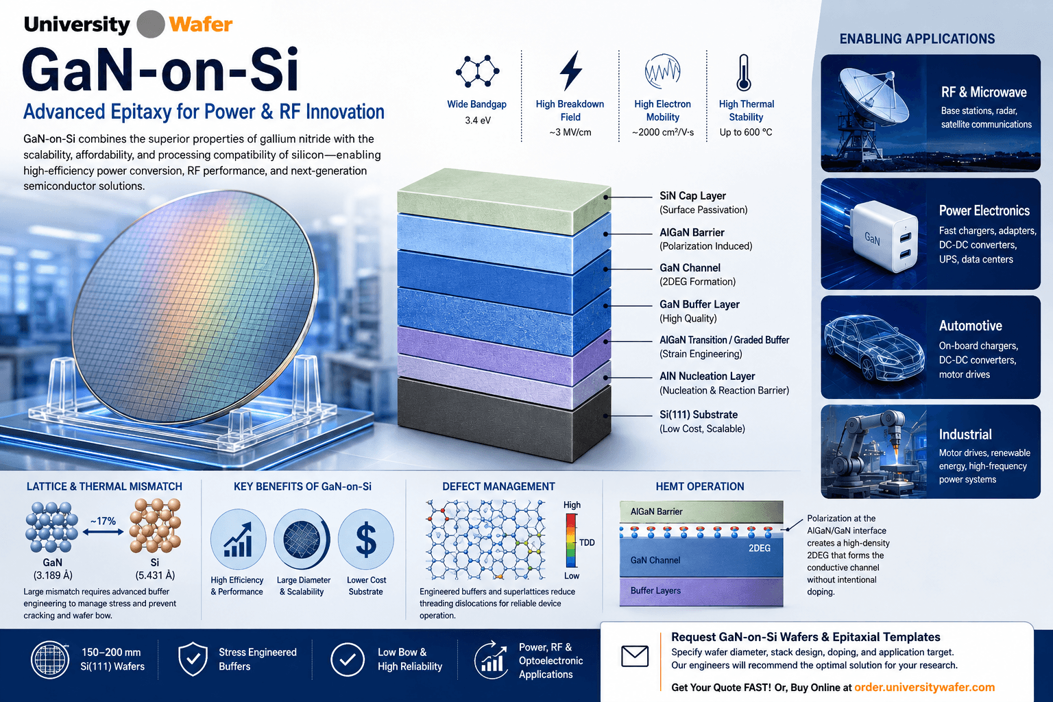
Unlike homoepitaxial growth, GaN growth on silicon requires carefully engineered intermediate layers because the two materials differ substantially in crystal structure, lattice dimensions, and thermal expansion behavior. Modern GaN-on-Si epitaxy therefore relies on nucleation, transition, and buffer layers that help control stress, cracking, defects, electrical leakage, and wafer bow.
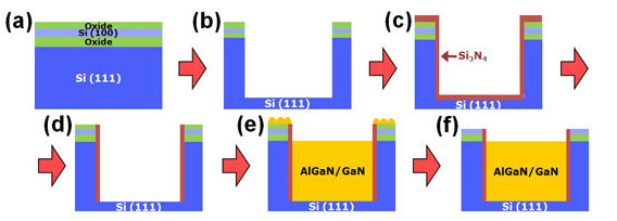
Why Is GaN-on-Silicon Epitaxy Challenging?
GaN and silicon are strongly mismatched materials. The lattice mismatch between GaN and Si is commonly cited at approximately 17%, while their different thermal expansion coefficients create additional stress when an epitaxial wafer cools from its growth temperature.
Because GaN contracts differently from silicon during cooldown, thick GaN layers grown without appropriate stress engineering can develop tensile stress, cracking, and wafer curvature. These effects become increasingly important as wafer diameter and total epitaxial thickness increase.
For this reason, successful GaN-on-Si growth normally incorporates AlN nucleation layers, AlGaN transition layers, superlattice structures, or other engineered buffer architectures between the silicon substrate and the active GaN device layers.
Typical GaN-on-Si Epitaxial Stack
The exact GaN-on-Si epitaxial structure depends on whether the wafer is intended for power, RF, HEMT, optoelectronic, or materials research. A representative AlGaN/GaN structure may include:
- Si(111) substrate: Provides a widely used silicon surface for III-nitride heteroepitaxy.
- AlN nucleation layer: Separates the Ga-containing epitaxy from the silicon surface, assists III-nitride nucleation, and can help suppress undesirable Ga-Si reactions.
- AlGaN transition or graded buffer layers: Used to engineer strain and help control cracking and wafer curvature.
- GaN buffer layer: Provides the foundation for the electrically active device structure.
- GaN channel: Forms the transport region in an AlGaN/GaN HEMT.
- AlGaN barrier: Creates the polarization discontinuity that helps form the two-dimensional electron gas at the AlGaN/GaN interface.
- Cap or passivation layer: Depending on the device design, SiN or other dielectric layers may be used to modify and stabilize surface and interface behavior.
AlN Nucleation Layers on Silicon
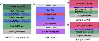
An aluminum nitride (AlN) nucleation layer is commonly used near the Si/GaN interface. Direct exposure of silicon to gallium at elevated epitaxial-growth temperatures can produce undesirable reactions, including melt-back etching under certain growth conditions.
An appropriately grown AlN layer helps establish the III-nitride surface required for subsequent buffer and GaN growth. AlN layer thickness, growth temperature, stress state, crystal quality, and interface preparation can all influence the resulting GaN film.
Researchers working with III-nitride buffer structures may also want to compare available aluminum nitride substrates and templates.
AlGaN Buffer Layers & Stress Engineering
AlGaN layers are frequently incorporated into GaN-on-Si buffer systems. By varying aluminum composition, layer thickness, and sequence, epitaxial engineers can modify the stress state developed during growth.
Step-graded AlGaN buffers and AlN/GaN or AlGaN/GaN multilayer structures are examples of approaches used to balance stress and improve the ability to grow thicker, crack-resistant GaN layers on silicon.
Buffer optimization is application-specific. A structure designed for a high-voltage power transistor may require different leakage, thickness, and stress characteristics than one designed for RF operation.
Why Si(111) Is Commonly Used
Si(111) is the most commonly used silicon orientation for conventional GaN-on-Si heteroepitaxy. Its surface symmetry is favorable for the nucleation of the basal plane of hexagonal wurtzite III-nitride layers.
Orientation alone does not eliminate the fundamental mismatch between GaN and silicon. Surface preparation and buffer engineering remain critical to obtaining usable epitaxial material.
Important silicon-substrate parameters may include:
- Wafer diameter
- Si(111) orientation and miscut
- Substrate thickness
- Resistivity
- Total thickness variation (TTV)
- Initial bow and warp
- Surface finish and cleanliness
See available Si(111) silicon wafers for epitaxial and semiconductor research.
How AlGaN/GaN HEMTs Work
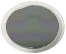
One of the most important GaN-on-Si device structures is the AlGaN/GaN high-electron-mobility transistor (HEMT). Wurtzite III-nitrides exhibit spontaneous and piezoelectric polarization. At an appropriately designed AlGaN/GaN heterointerface, the resulting polarization discontinuity can support a high-density two-dimensional electron gas (2DEG) near the interface.
The 2DEG provides the conductive transistor channel without requiring conventional intentional donor doping of the channel itself. Its properties depend on factors including barrier composition, barrier thickness, strain, interface quality, surface conditions, and device processing.
Learn more about GaN HEMT wafers and HEMT transistor substrates.
GaN-on-Si for Power Electronics
GaN's wide bandgap and high critical electric field make III-nitride heterostructures attractive for high-voltage, high-frequency power switching. Lateral GaN HEMTs can operate with fast switching transitions while maintaining comparatively low conduction losses when appropriately designed.
GaN power devices are used or investigated for applications including:
- AC/DC and DC/DC power conversion
- Compact fast chargers and adapters
- Data-center power supplies
- Telecommunications power conversion
- Automotive power electronics
- Industrial power systems
- High-frequency power-conversion research

GaN-on-Si for RF Devices
GaN HEMTs are also important in RF and microwave electronics because the AlGaN/GaN system can combine high carrier density, high electric-field capability, and high-frequency transistor operation.
Depending on substrate and device requirements, GaN RF technology is investigated and deployed in applications such as:
- RF power amplifiers
- Wireless infrastructure
- Radar systems
- Satellite and microwave communications
- High-frequency laboratory devices
For applications in which heat extraction and very high RF power density are primary concerns, GaN-on-SiC and silicon carbide substrates are also important platforms to compare.
Defects in GaN-on-Silicon
Because GaN-on-Si is a heteroepitaxial material system, defects such as threading dislocations can propagate through the epitaxial layers. Their density and electrical significance depend strongly on the nucleation process, buffer structure, total thickness, growth conditions, and device design.
Buffer layers and strain-management structures can alter dislocation propagation and reduce cracking, but they do not eliminate every crystal defect. For this reason, material characterization should be matched to the intended application rather than relying on a single defect-density number.
Wafer Bow, Warp & Stress Control
Wafer bow is an important parameter for large-diameter GaN-on-Si wafers because excessive curvature can complicate lithography, wafer handling, deposition, bonding, and other downstream processes.
Bow depends on the complete epitaxial structure, including layer thicknesses, composition, growth temperature, residual stress, and substrate thickness. Consequently, an acceptable bow specification should be defined for the actual wafer diameter, epitaxial stack, and process equipment rather than assumed from a universal value.
Electrical Isolation & Buffer Leakage
The buffer beneath a GaN HEMT must provide both structural support and appropriate electrical isolation. Unwanted conduction through the buffer can increase off-state leakage and reduce device performance.
Carbon-doped GaN buffers are widely investigated and used for increasing buffer resistivity in GaN power-device structures. Other compensation approaches may also be used depending on the epitaxial technology and application.
Buffer doping must be carefully engineered because the same defects and deep levels that help suppress leakage can also contribute to trapping phenomena and dynamic device behavior.
Trapping & Dynamic RON
Charge trapping is an important reliability consideration in AlGaN/GaN HEMTs. Traps may be associated with surfaces, interfaces, dielectric layers, structural defects, or the buffer region. Charge captured during high-field operation can temporarily alter the conductivity of the device.
One resulting phenomenon is an increase in dynamic RON after high-voltage stress, sometimes associated with current collapse. Device designers therefore investigate surface passivation, field plates, buffer design, gate structures, and processing conditions to manage trapping effects.
Surface Passivation & Field Plates
Dielectric passivation layers such as SiN are commonly used in GaN HEMT fabrication to modify surface-state behavior and protect the semiconductor surface. Other dielectric materials, including Al2O3, are also investigated for gate and surface interfaces.
Field plates are another important device-design technique. By redistributing the electric field near the gate-drain region, an appropriately designed field plate can reduce localized electric-field peaks and influence breakdown and dynamic behavior.
Thermal Management of GaN-on-Si
Heat removal is important in both power and RF GaN devices. Silicon has substantially higher bulk thermal conductivity than sapphire at room temperature, but lower bulk thermal conductivity than silicon carbide. The actual thermal resistance of a GaN device also depends on the III-nitride buffer stack, interfaces, die thickness, metallization, package, and cooling method.
Consequently, substrate thermal conductivity alone should not be used to predict device junction temperature or long-term reliability.
MOCVD Growth of GaN-on-Silicon
Metal-organic chemical vapor deposition (MOCVD) is one of the principal techniques used to grow GaN and AlGaN epitaxial layers for commercial III-nitride semiconductor structures.
Precise control of precursor delivery, temperature, pressure, V/III ratio, layer composition, and growth sequence is required because each portion of the GaN-on-Si stack influences stress, crystal quality, interfaces, and electrical performance.
Characterizing GaN-on-Si Epitaxial Wafers
No single measurement fully describes the quality of a GaN-on-Si wafer. Researchers typically combine structural, surface, electrical, and wafer-level measurements according to the intended device.
- X-ray diffraction (XRD): Evaluates epitaxial orientation, strain, and crystalline characteristics.
- Atomic force microscopy (AFM): Measures surface morphology and nanoscale roughness.
- Hall measurements: Determine sheet carrier concentration and mobility when an appropriate conductive heterostructure is present.
- C–V measurements: Provide information about charge and electrostatic behavior.
- Wafer bow and warp: Characterize macroscopic wafer curvature.
- Electrical leakage measurements: Evaluate isolation and buffer behavior.
- Pulsed I–V and dynamic testing: Help characterize trapping and current-collapse phenomena in fabricated devices.
GaN-on-Si vs GaN-on-SiC vs GaN-on-Sapphire
GaN can be grown on several foreign substrate materials, and there is no universally best platform. Selection depends on device type, thermal requirements, wafer diameter, process infrastructure, performance targets, and cost.
- GaN-on-Si: Attractive for larger-diameter processing, silicon manufacturing infrastructure, and power-device development. Stress and buffer engineering are especially important.
- GaN-on-SiC: Silicon carbide provides high thermal conductivity and is an important substrate platform for high-power-density RF GaN devices.
- GaN-on-Sapphire: Sapphire-based GaN is extensively used for III-nitride optoelectronics and is also used in electronic-device research.
Emerging GaN-on-Si Research
Research continues into higher-voltage GaN devices, improved buffer architectures, normally-off HEMTs, heterogeneous integration, advanced thermal management, wafer-level packaging, and integration of GaN power stages with silicon-based control electronics.
These approaches seek to combine GaN's device-level advantages with mature silicon processing and packaging technologies while addressing challenges involving stress, defects, thermal resistance, trapping, and electrical isolation.
GaN-on-Si Wafer Specifications to Consider
When sourcing a GaN-on-Si epitaxial wafer, researchers should define specifications according to the intended device or experiment. Useful parameters may include:
- Silicon wafer diameter and orientation
- Substrate thickness and resistivity
- AlN nucleation-layer structure
- Buffer composition and total thickness
- GaN channel thickness
- AlGaN barrier composition and thickness
- Intentional buffer doping or compensation
- Cap or passivation requirements
- Wafer bow, warp, and TTV
- Surface morphology
- Target power, RF, HEMT, or materials-research application
Request GaN-on-Si Wafers & Epitaxial Structures
UniversityWafer can assist researchers sourcing GaN-on-Si wafers, Si(111) substrates, AlGaN/GaN structures, and related wide-bandgap semiconductor materials. Provide your required wafer diameter, substrate specifications, epitaxial structure, electrical requirements, and intended application when requesting availability.