
III-V Semiconductor Wafers for High-Performance Devices
III-V semiconductors are compound semiconductor materials formed primarily from elements in Group 13 and Group 15 of the periodic table. Important examples include gallium arsenide (GaAs), indium phosphide (InP), indium arsenide (InAs), gallium antimonide (GaSb), gallium phosphide (GaP), and the III-nitride material gallium nitride (GaN).
These materials provide electronic and optical properties that make them important for applications where conventional silicon does not provide the required combination of carrier transport, optical emission, absorption wavelength, breakdown field, or high-frequency performance. UniversityWafer supplies III-V semiconductor wafers and substrates for RF electronics, photonics, optoelectronics, infrared detection, power electronics, solar cells, and quantum-device research.
Why Are III-V Semiconductors Important?
There is no single property shared by every III-V material that makes it universally superior to silicon. Instead, different III-V compounds are selected because their band structure, carrier transport, breakdown characteristics, and optical properties can provide important advantages for specific devices.
Many important III-V semiconductors, including GaAs and InP, have direct bandgaps. Direct-bandgap materials can efficiently couple electronic transitions to photons, making them particularly useful for LEDs, semiconductor lasers, photodetectors, and other optoelectronic devices.
Several III-V materials also provide high electron mobility or high electron saturation velocity, which can be advantageous for high-frequency and high-speed transistor technologies.
Gallium Arsenide (GaAs) for RF & Optoelectronics
Gallium arsenide (GaAs) wafers are widely used in high-frequency electronics and optoelectronics. GaAs has a direct bandgap of approximately 1.42 eV at room temperature and substantially higher electron mobility than silicon under comparable low-field conditions.
These properties make GaAs and GaAs-based heterostructures useful for RF amplifiers, microwave devices, laser diodes, LEDs, photodetectors, and high-efficiency solar cells. Semi-insulating GaAs substrates are particularly valuable for RF integrated circuits because their high substrate resistivity can help reduce parasitic conduction.
GaAs is also an important substrate for epitaxial compound-semiconductor systems such as AlGaAs/GaAs and InGaP/GaAs heterostructures.
Indium Phosphide (InP) for High-Speed Photonics
Indium phosphide (InP) wafers provide an important substrate platform for high-speed electronics, photonic integrated circuits, lasers, modulators, and photodetectors. InP is a direct-bandgap III-V semiconductor with a room-temperature bandgap of approximately 1.34 eV.
One of the major advantages of InP is its compatibility with InGaAs/InGaAsP heterostructures. These material systems can be engineered for wavelengths important to fiber-optic telecommunications, including the approximately 1.3 µm and 1.55 µm spectral regions.
As a result, InP-based technologies are important for optical communications, photonic integrated circuits (PICs), high-speed photodetectors, semiconductor lasers, and high-frequency transistors.
Gallium Nitride (GaN) for Power & RF Devices
Gallium nitride (GaN) is a wide-bandgap III-V semiconductor with a bandgap of approximately 3.4 eV for wurtzite GaN at room temperature. Its high critical electric field and favorable high-frequency characteristics make GaN important for power conversion and RF electronics.
GaN-based heterostructures, particularly AlGaN/GaN structures, are used to fabricate high-electron-mobility transistors (HEMTs). These devices exploit a high-density two-dimensional electron gas near the heterointerface and are widely investigated and used for RF and high-power electronic applications.
GaN is also a foundational material for blue and ultraviolet optoelectronics. GaN and related InGaN/AlGaN alloys are used in LEDs, laser diodes, UV devices, and other advanced optoelectronic structures.
GaN-on-Sapphire, GaN-on-Si & GaN-on-SiC
GaN devices are frequently fabricated using heteroepitaxial structures because large native GaN substrates have historically been more difficult and costly to produce than conventional semiconductor wafers.
Common platforms include GaN-on-sapphire , GaN-on-silicon, and GaN-on-SiC. Each substrate presents different tradeoffs involving cost, thermal transport, wafer size, electrical properties, lattice mismatch, thermal-expansion mismatch, and integration with existing fabrication processes.
Sapphire is extensively used for GaN LEDs and optoelectronics. Silicon can provide larger wafer formats and potential compatibility with established semiconductor infrastructure, while SiC offers high thermal conductivity that is particularly valuable for high-power-density RF GaN devices.
Indium Arsenide (InAs) for Infrared & Quantum Devices
Indium arsenide (InAs) substrates are narrow-bandgap III-V semiconductors known for very high electron mobility and strong infrared response.
These properties make InAs important for infrared detectors, high-speed electronics, terahertz research, Hall devices, quantum structures, and low-dimensional semiconductor systems.
InAs is also widely studied in semiconductor nanostructures and heterostructures. For example, self-assembled InAs quantum dots can be formed in appropriate epitaxial systems such as InAs/GaAs, enabling research in quantum optics, photonics, lasers, and quantum information technologies.
Gallium Antimonide (GaSb) for Infrared Devices
Gallium antimonide (GaSb) wafers provide a substrate platform for narrow-bandgap III-V semiconductor heterostructures used in infrared technologies.
GaSb-based material systems are important for mid-infrared photodetectors, infrared lasers, thermophotovoltaic devices, and advanced optoelectronic research. Alloys and heterostructures involving InAs, AlSb, InGaSb, and related compounds can be engineered for specific infrared wavelength ranges and electronic properties.
III-V Heterostructures & Bandgap Engineering
One of the most important advantages of III-V semiconductor technology is the ability to combine different compound semiconductors into heterostructures. By controlling material composition and layer thickness, researchers can engineer band offsets, quantum confinement, carrier transport, and optical transition energies.
Important III-V heterostructure systems include AlGaAs/GaAs, InGaAs/InP, InGaAsP/InP, AlGaN/GaN, and InGaP/GaAs. InGaP/GaAs epitaxial structures , for example, are used in heterojunction bipolar transistors (HBTs), optoelectronics, and multijunction photovoltaic devices.
Heterostructure design must account for lattice constants, strain, thermal-expansion behavior, band alignment, interface quality, doping, and defect formation.
III-V Materials for HEMT Devices
High-electron-mobility transistors (HEMTs) use semiconductor heterojunctions to create a high-mobility carrier channel. III-V heterostructures are especially suitable for HEMTs because their band offsets and carrier transport properties can be engineered through epitaxial layer design.
GaAs-based HEMTs and GaN-based HEMTs are used in different portions of the RF and microwave market. GaAs technologies can provide excellent low-noise and high-frequency performance, while GaN HEMTs are especially attractive where high RF power density and high breakdown capability are required.
III-V Semiconductor Lasers & LEDs
Direct-bandgap III-V semiconductor systems are foundational materials for modern solid-state light sources. Electrons and holes can recombine radiatively in the active region, producing photons with energies determined by the semiconductor band structure.
By changing alloy composition and heterostructure design, III-V devices can be engineered across a broad range of wavelengths. GaN/InGaN systems are important for blue and ultraviolet emitters, while GaAs-, InP-, and GaSb-based systems support visible, near-infrared, and infrared optoelectronic technologies.
III-V Wafers for Photodetectors
III-V photodetectors convert incident optical radiation into an electrical response. Selecting the semiconductor bandgap is critical because it determines which photon energies can be absorbed efficiently.
GaAs is useful for visible and near-infrared detection, InGaAs grown on InP is widely used for near-infrared telecommunications and sensing, and narrow-bandgap materials such as InAs, InSb, and GaSb-based heterostructures extend detection farther into the infrared.
III-V Semiconductors for High-Efficiency Solar Cells
III-V materials are also important for high-efficiency photovoltaic devices. GaAs is an excellent photovoltaic absorber because of its direct bandgap and strong optical absorption.
Multijunction solar cells combine semiconductor layers with different bandgaps so that different portions of the solar spectrum can be converted more efficiently than with a single-junction device. III-V alloys such as InGaP, GaAs, and related compounds are widely used in high-performance multijunction architectures, particularly for space and concentrator photovoltaic applications.
Researchers can learn more about GaAs solar cell substrates for advanced photovoltaic research.
III-V Integration with Silicon & SOI
Integrating III-V semiconductors with silicon wafers or silicon-on-insulator (SOI) wafers is an important research area because it can combine the mature fabrication infrastructure of silicon with the optical and electronic properties of III-V materials.
Integration approaches can include direct epitaxial growth, wafer or die bonding, transfer techniques, and other heterogeneous-integration processes. Direct III-V growth on silicon can be challenging because lattice mismatch, thermal-expansion differences, polarity effects, and crystalline defects can degrade material and device performance.
Despite these challenges, integrated silicon III-V devices are being developed for silicon photonics, optical communications, high-speed electronics, RF systems, and other advanced integrated technologies.
Selecting a III-V Semiconductor Substrate
Choosing the correct III-V wafer requires matching the substrate properties to the intended device and epitaxial structure. Important specifications can include:
- Material: GaAs, InP, InAs, GaSb, GaP, GaN, InSb, or another III-V compound
- Crystal orientation: selected according to epitaxy and device-processing requirements
- Doping: n-type, p-type, undoped, or semi-insulating where available
- Carrier concentration and resistivity: selected for the required electrical behavior
- Thickness and diameter: matched to processing and equipment requirements
- Surface finish: including polished and epi-ready surfaces when required
- Offcut or misorientation: important for some epitaxial growth processes
- Defect density: particularly important for demanding epitaxial and device applications
Careful substrate selection provides a reliable starting platform for III-V semiconductor devices, RF electronics, photonics, optoelectronics, power electronics, infrared detectors, solar cells, and quantum-device research.
Get Your III-V Semiconductor Wafer Quote FAST! Or, Buy Wafers Online and Start Researching Today!
High-Performance III-V Semiconductor Devices
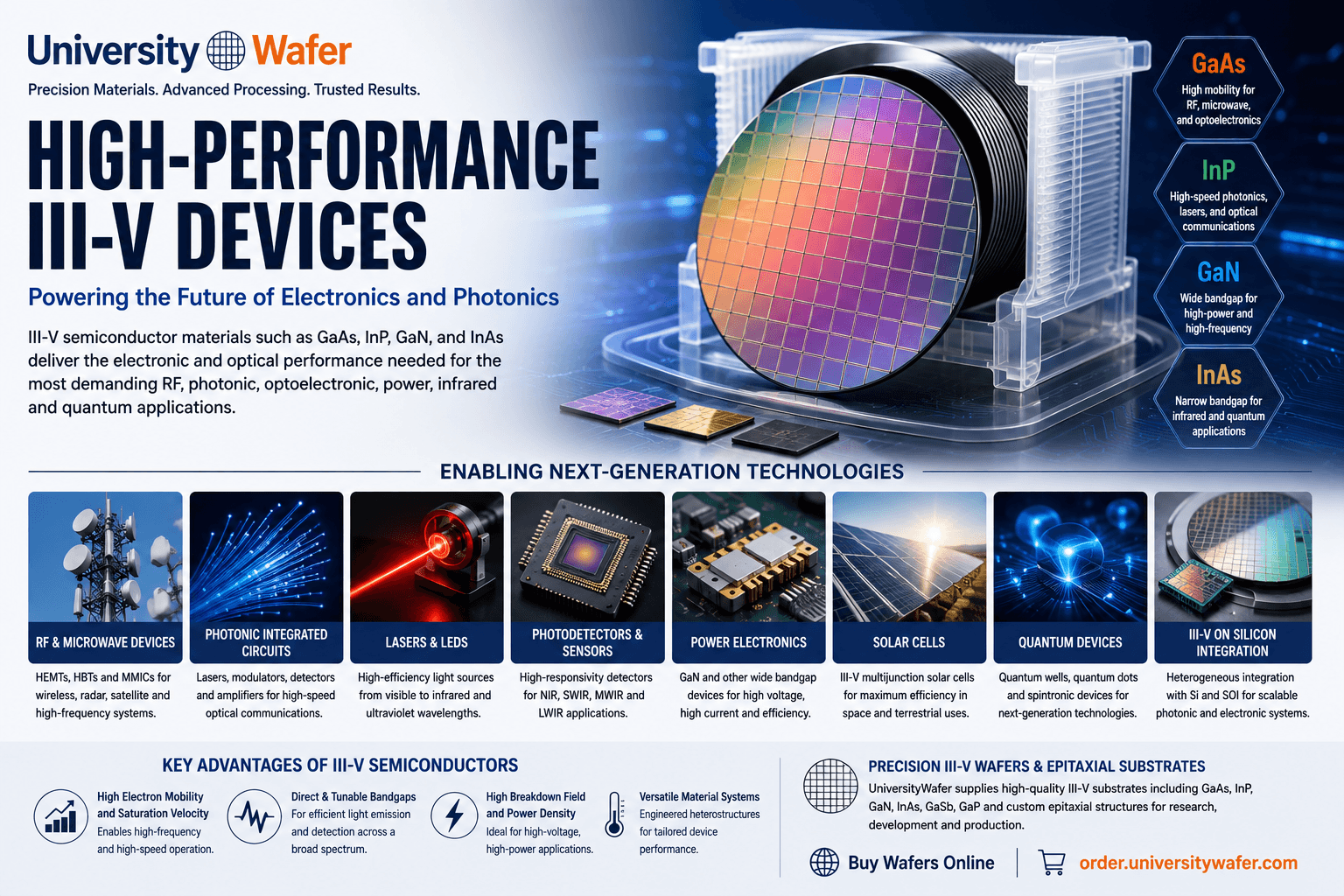
III-V semiconductor devices are used when an application requires electronic or optical properties that are difficult to achieve with conventional silicon alone. Depending on the material system, III-V semiconductors can provide direct bandgaps, high electron mobility, high electron saturation velocity, wide-bandgap operation, or strong infrared response.
These properties support advanced technologies including RF and microwave transistors, semiconductor lasers, LEDs, photodetectors, photonic integrated circuits, power devices, solar cells, infrared sensors, and quantum structures.
UniversityWafer supplies III-V semiconductor wafers including GaAs, InP, InAs, GaSb, GaP, InSb, GaN, and related compound semiconductor materials for research and device development.
III-V Epitaxy for Advanced Semiconductor Devices
Many high-performance III-V devices depend on precisely controlled epitaxial semiconductor layers. Epitaxy allows crystalline layers with engineered composition, thickness, doping, and band structure to be grown on an appropriate crystalline substrate.
Techniques such as molecular beam epitaxy (MBE) and metal-organic chemical vapor deposition (MOCVD) are widely used to fabricate III-V heterostructures, quantum wells, superlattices, and device layers.
Epitaxial quality depends strongly on substrate orientation, surface preparation, lattice matching, growth temperature, composition, and defect density. Excessive lattice mismatch can generate strain and, above certain conditions, defects such as misfit and threading dislocations.
III-V Heterostructures & Band Engineering
A major advantage of compound semiconductor technology is the ability to create III-V heterostructures by combining materials with different bandgaps and band-edge energies. This allows engineers to control carrier confinement, charge transport, optical transitions, and electric-field distributions within a device.
Examples include AlGaAs/GaAs, InGaAs/InP, InGaAsP/InP, AlGaN/GaN, InGaP/GaAs, and InAs/AlSb-based systems. Alloy composition can be adjusted to engineer bandgap energy and, within material-system constraints, lattice constant.
These heterostructures form the foundation of many HEMTs, HBTs, semiconductor lasers, photodetectors, quantum wells, and high-efficiency photovoltaic devices.
HEMTs for RF & Microwave Electronics
High-electron-mobility transistors (HEMTs) use a semiconductor heterojunction to form a high-mobility conduction channel. III-V HEMTs are important for RF, microwave, millimeter-wave, satellite, radar, and wireless communication systems.
GaAs-based HEMTs and pseudomorphic HEMTs have long been used for low-noise and high-frequency electronics. InP-based HEMTs can provide extremely high-frequency performance, while AlGaN/GaN HEMTs combine high-frequency operation with high breakdown capability and high power density.
Researchers developing nitride-based devices can explore GaN semiconductor substrates for RF, power, LED, and advanced III-V device research.
III-V Heterojunction Bipolar Transistors
Heterojunction bipolar transistors (HBTs) use semiconductor materials with different bandgaps in the emitter, base, or collector regions. Proper heterojunction design can improve carrier injection and enable excellent high-frequency performance.
Important III-V HBT technologies include AlGaAs/GaAs, InGaP/GaAs, and InP/InGaAs material systems. These devices are used in RF power amplifiers, wireless communications, high-speed electronics, optical communication circuits, and other microwave applications.
InP for Photonic Integrated Circuits
Indium phosphide (InP) wafers are particularly important for photonic integrated circuits (PICs). InP-based heterostructures can integrate active optical components such as lasers, semiconductor optical amplifiers, modulators, and photodetectors on a common semiconductor platform.
InGaAs and InGaAsP layers lattice matched or appropriately engineered with InP are especially useful for devices operating near the telecommunications wavelength regions around 1.3 µm and 1.55 µm.
These material systems support fiber-optic communications, optical interconnects, sensing, LiDAR research, spectroscopy, and high-speed photonic systems.
GaAs for High-Frequency RF Devices
Gallium arsenide (GaAs) wafers remain important for RF and microwave electronics because GaAs provides high electron mobility and can be produced as semi-insulating substrates.
Semi-insulating GaAs can provide electrical isolation between devices and reduce conductive substrate losses in appropriate microwave integrated circuits. GaAs technologies are used in RF amplifiers, low-noise amplifiers, microwave circuits, satellite communications, and other high-frequency systems.
GaN for High-Power RF Electronics
GaN differs from GaAs and InP because its wide bandgap and high critical electric field make it particularly attractive for devices requiring high voltage or high RF power density.
AlGaN/GaN HEMTs are used in RF power amplifiers, radar, satellite communications, base-station infrastructure, and other high-frequency systems. The substrate underneath the GaN epitaxial structure also influences thermal management and device fabrication.
GaN-on-sapphire , GaN-on-Si, GaN-on-SiC, and native GaN substrates each provide different combinations of cost, thermal conductivity, wafer availability, lattice relationship, and process compatibility.
III-V Materials for Infrared Detection
Narrow-bandgap III-V materials are particularly important for infrared photodetectors. The semiconductor bandgap influences the longest photon wavelength that can generate electron-hole pairs through band-to-band absorption.
Indium arsenide (InAs) , InSb, InGaAs, and GaSb-based heterostructures are used across different infrared wavelength ranges. Applications include thermal sensing, spectroscopy, gas detection, imaging, communications, and scientific instrumentation.
Gallium antimonide (GaSb) substrates are particularly useful as platforms for infrared heterostructures involving compounds such as InAs, AlSb, and related alloys.
III-V Semiconductor Lasers
Direct-bandgap III-V materials are fundamental to semiconductor laser technology. Quantum wells and heterostructures can confine electrons, holes, and optical fields, improving the efficiency and control of stimulated emission.
GaAs-based materials support visible and near-infrared laser systems, while InP-based compounds are important for telecommunications and near-infrared photonics. GaSb-based systems can extend semiconductor laser operation farther into the infrared, while III-nitride materials support blue and ultraviolet emission.
III-V LEDs & Light-Emitting Devices
III-V semiconductor alloys enable LEDs across a broad spectral range. InGaN/GaN structures are central to blue and green LEDs, while AlGaInP-based structures are widely used for efficient red, orange, and yellow emission.
Material composition, quantum-well structure, strain, doping, defects, and optical extraction all influence LED efficiency. Substrate selection is therefore closely connected to epitaxial growth and final device performance.
III-V Multijunction Solar Cells
III-V semiconductor materials are used to produce some of the highest-efficiency photovoltaic devices. In a multijunction solar cell, multiple semiconductor junctions with different bandgaps absorb different portions of the solar spectrum.
GaAs and alloys such as InGaP are important components of these architectures. Carefully engineered junctions can reduce energy losses compared with a single-junction cell, although device fabrication is significantly more complex.
Learn more about GaAs substrates for high-efficiency solar cells and compound-semiconductor photovoltaic research.
III-V Quantum Wells & Quantum Dots
III-V heterostructures can confine charge carriers in structures with dimensions comparable to their quantum-mechanical length scales. Quantum wells provide confinement in one spatial dimension, while quantum dots provide stronger three-dimensional confinement.
InAs quantum dots in GaAs-based structures are widely studied for quantum optics, single-photon sources, semiconductor lasers, and other quantum technologies. III-V quantum wells are similarly important in lasers, modulators, detectors, HEMTs, and high-speed optoelectronics.
Integrating III-V Devices with Silicon Photonics
Silicon provides a mature and scalable fabrication platform, but its indirect bandgap makes efficient electrically pumped light emission difficult. Integrating III-V materials with silicon can combine silicon-based waveguides and fabrication infrastructure with efficient III-V optical gain and detection.
III-V integration with silicon-on-insulator (SOI) wafers can be achieved through techniques such as wafer bonding, die bonding, transfer printing, or carefully engineered direct epitaxial growth.
Direct heteroepitaxy is challenging because lattice mismatch, thermal-expansion mismatch, and polar/nonpolar interface effects can generate defects. Heterogeneous bonding avoids some epitaxial constraints and is therefore important for integrated III-V/silicon photonics.
Lattice Matching in III-V Heterostructures
Lattice matching is an important consideration when growing one crystalline III-V material on another. If the natural lattice constants differ, the epitaxial layer may initially accommodate the mismatch through elastic strain.
When the layer exceeds a composition- and structure-dependent critical thickness, strain relaxation can occur through defects such as misfit dislocations. These defects can propagate through the device structure and adversely affect electrical or optical performance.
Researchers therefore carefully select substrate materials, alloy compositions, buffer layers, growth conditions, and layer thicknesses when designing high-performance III-V heterostructures.
Thermal Management in High-Performance III-V Devices
Thermal management is critical for high-power and high-frequency semiconductor devices. Junction temperature can affect carrier mobility, reliability, output power, optical efficiency, and device lifetime.
Different III-V substrates have substantially different thermal properties. GaAs and InP, for example, generally conduct heat less effectively than high-quality silicon carbide. This is one reason GaN-on-SiC is attractive for high-power-density RF applications.
Device designers must consider the complete thermal path, including epitaxial layers, substrate thickness, interfaces, metallization, packaging, heat spreaders, and operating conditions.
Surface Quality for III-V Epitaxy
High-quality epitaxial growth requires carefully prepared substrate surfaces. Surface contamination, native oxides, polishing damage, particles, scratches, and excessive roughness can interfere with nucleation and epitaxial layer quality.
Epi-ready III-V wafers are prepared to provide surfaces suitable for subsequent epitaxial processing. Required specifications depend on the material, growth system, device architecture, and epitaxy technique.
III-V Wafer Orientation & Offcut
Crystallographic orientation can influence epitaxial growth, surface reconstruction, step formation, etching behavior, and device processing. III-V wafers may therefore be specified with an exact nominal orientation or a controlled offcut toward a particular crystallographic direction.
The appropriate orientation and misorientation depend on the substrate material and epitaxial process. Researchers should specify these parameters when they are important to growth morphology or device performance rather than assuming the same orientation is optimal for every III-V system.
Custom III-V Semiconductor Wafers
UniversityWafer supplies custom III-V semiconductor substrates for photonics, RF electronics, optoelectronics, power devices, infrared sensing, solar cells, and quantum-device research.
Important specifications can include:
- Material: GaAs, InP, InAs, GaSb, GaP, InSb, GaN, or related compounds
- Wafer diameter and thickness
- Crystal orientation and offcut
- Doping type and dopant species
- Carrier concentration or resistivity
- Semi-insulating or conductive substrate requirements
- Single-side or double-side polish
- Surface roughness and epi-ready preparation
- Epitaxial layer composition and thickness, when required
- Defect-density requirements for demanding applications
Matching these specifications to the intended device provides a more reliable foundation for high-performance III-V semiconductor devices and advanced compound-semiconductor research.
III-V Materials for Next-Generation Technology
No single III-V semiconductor is optimal for every high-performance application. GaAs is important for RF and optoelectronic devices, InP supports high-speed photonics and telecommunications, GaN provides wide-bandgap performance for RF power and power electronics, and InAs, InSb, and GaSb-based materials extend device capabilities into infrared and quantum technologies.
Selecting the appropriate substrate, epitaxial structure, doping, orientation, and surface preparation allows researchers to exploit the particular advantages of each compound semiconductor material.
Related III-V Semiconductor Resources
- III-V Semiconductor Wafers & Substrates
- Gallium Arsenide (GaAs) Wafers
- Indium Phosphide (InP) Wafers
- Indium Arsenide (InAs) Substrates
- Gallium Antimonide (GaSb) Wafers
- Gallium Nitride (GaN) Substrates
- GaN-on-Sapphire Wafers
- Gallium Phosphide (GaP) Wafers
- Molecular Beam Epitaxy (MBE)
- InGaP/GaAs Epitaxial Structures
- GaAs Wafers for High-Efficiency Solar Cells
- Integrated Silicon & III-V Semiconductor Devices
- SOI Wafers for III-V Integration & Photonics
- Silicon Wafers for III-V Integration
- Semiconductor Wafers & Substrates