
How Are Semiconductor Devices Manufactured?
Semiconductor device manufacturing uses a sequence of highly controlled processes to create electronic structures on or within a semiconductor wafer. Silicon is the dominant substrate for conventional integrated circuits, although materials such as gallium arsenide (GaAs), silicon carbide (SiC), and gallium nitride (GaN) are important for applications requiring properties such as high-frequency operation, optoelectronic functionality, or high-power performance.
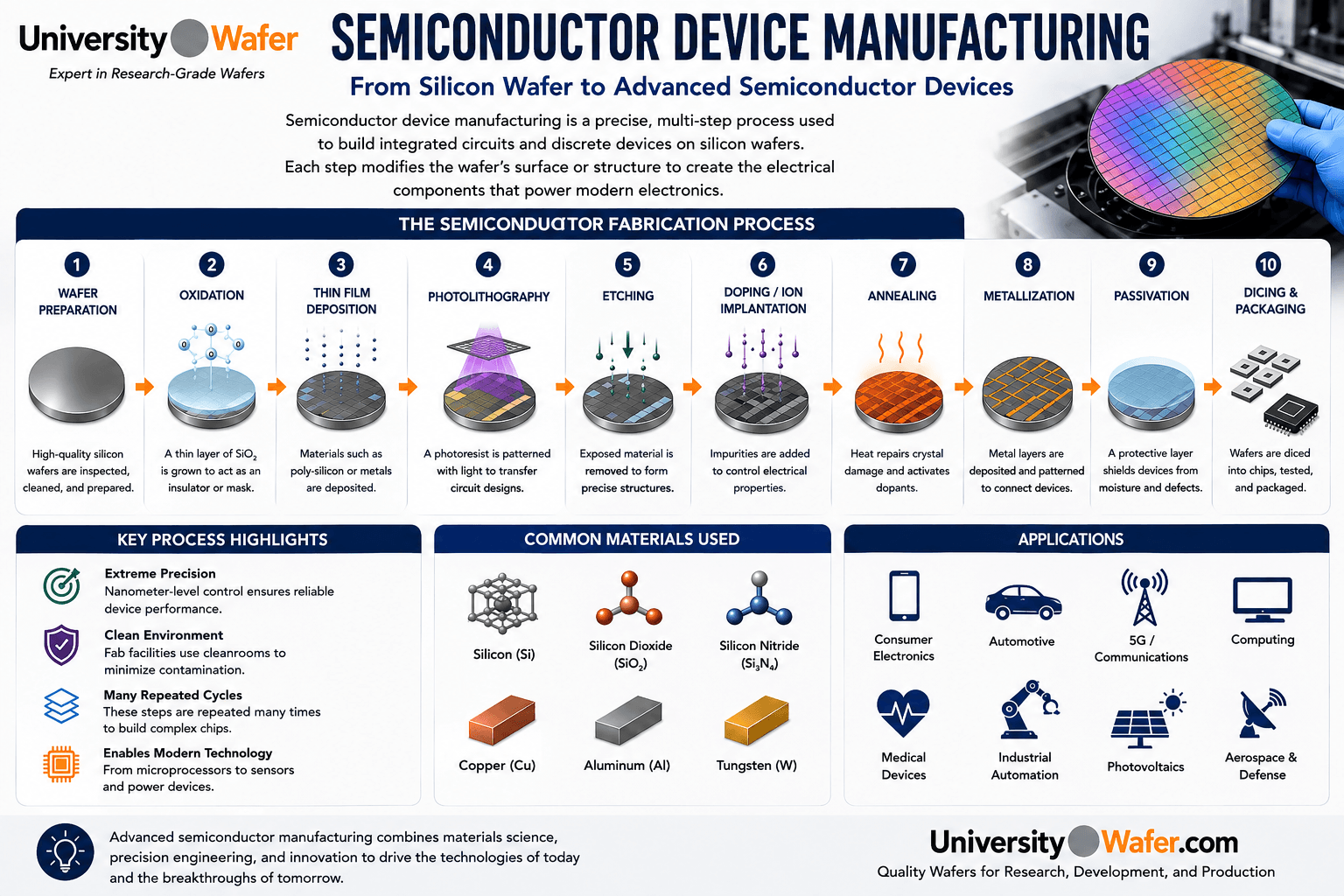
Modern wafer fabrication does not consist of a single manufacturing step. Instead, deposition, lithography, etching, doping, cleaning, and thermal processing may be repeated many times to build transistors, interconnects, dielectric structures, sensors, and other device features.
Semiconductor Wafer Preparation
Device fabrication begins with a substrate whose properties are appropriate for the intended process. For silicon technology, important specifications can include crystal orientation, conductivity type, resistivity, diameter, thickness, surface finish, flatness, and defect requirements.
High-quality silicon wafers are commonly produced from single-crystal ingots grown by the Czochralski (CZ) process or float-zone methods. After crystal growth, ingots are sliced into wafers and undergo operations such as edge shaping, lapping or grinding, cleaning, etching, and polishing to obtain the required geometry and surface condition.
Thermal Oxidation and Dielectric Layers
Silicon has an important technological advantage because a high-quality silicon dioxide (SiO2) layer can be thermally grown directly from the silicon surface. During thermal oxidation, silicon reacts with an oxidizing species at elevated temperature to form SiO2.
Thermal oxide can serve as an electrical insulator, surface-passivation layer, masking material, or part of a dielectric stack, depending on the device and fabrication process. Other dielectric materials, including silicon nitride and deposited oxides, are also widely used in semiconductor processing.
Thin-Film Deposition
Thin-film deposition adds controlled layers of conducting, semiconducting, or insulating materials to the wafer. Common techniques include chemical vapor deposition (CVD), physical vapor deposition (PVD), atomic layer deposition (ALD), and epitaxial growth.
The appropriate deposition technique depends on requirements such as film composition, thickness, conformality, crystallinity, interface quality, deposition temperature, and allowable thermal budget. For example, TEOS-based oxide deposition can be used to form silicon oxide films, while silicon nitride is used for applications including dielectric isolation, passivation, masking, and mechanical structures.
Photolithography and Pattern Transfer
Photolithography defines patterns that determine where subsequent fabrication processes modify the wafer. A photosensitive resist is applied to the surface, exposed through a mask or reticle using suitable radiation, and developed to produce a patterned resist layer.
The resulting pattern can protect selected regions while other areas undergo processes such as etching, implantation, or deposition. Lithography and pattern transfer are repeated throughout semiconductor fabrication to construct multiple device and interconnect levels.
Wet and Dry Etching
Semiconductor etching selectively removes material from exposed regions of a wafer. Wet etching uses liquid chemical solutions, while dry etching uses gas-phase chemistry and often plasma-assisted reactions.
Some wet etchants exhibit crystallographic selectivity when used with single-crystal silicon. This behavior is important in anisotropic silicon etching, where the etch rate depends strongly on crystal orientation and can be used to form orientation-dependent structures for MEMS and microfabrication.
Doping Semiconductor Wafers
Semiconductor doping intentionally introduces electrically active impurities to control carrier concentration and conductivity. In silicon, acceptor dopants such as boron are commonly used to produce p-type silicon, while donor dopants such as phosphorus or arsenic can produce n-type material.
Localized doped regions may be formed by processes such as ion implantation or thermal diffusion. Ion implantation accelerates dopant ions into the wafer and provides control over dose and depth distribution. A subsequent thermal treatment is commonly required to repair implantation-induced crystal damage and electrically activate dopants by incorporating them into appropriate lattice sites.
Why Wafer Specifications Matter
Semiconductor manufacturing performance depends not only on processing equipment but also on the starting substrate. Parameters including wafer orientation, resistivity, doping type, thickness, surface roughness, total thickness variation, bow, and surface cleanliness can affect processing and experimental results.
UniversityWafer supplies semiconductor wafers and research substrates for semiconductor device fabrication, process development, university laboratories, MEMS, thin-film research, and other microfabrication applications.
Get Your Semiconductor Wafer Quote FAST!
Or,
Buy Wafers Online
and Start Researching Today!
Chemical Mechanical Polishing and Planarization
As semiconductor devices are built through repeated deposition, patterning, and etching steps, the wafer surface can develop significant topography. Chemical Mechanical Polishing (CMP) is used to planarize selected layers and restore a sufficiently flat surface for subsequent processing.
CMP combines controlled chemical reactions with mechanical abrasion. The process typically uses a polishing pad and chemically formulated slurry containing abrasive particles. Process chemistry, pad properties, pressure, relative motion, and material selectivity are controlled to achieve the required removal rate and surface condition.
Planarization is especially important in multilayer semiconductor structures because excessive surface topography can complicate lithography and subsequent film formation. CMP is used in processes involving dielectric materials, metals, and other layers, with the exact slurry and process conditions selected for the materials being polished.
Metallization and Electrical Interconnects
After active semiconductor structures have been formed, conductive pathways are required to electrically connect transistors and other device elements. Semiconductor metallization creates these interconnects using patterned conductive layers separated by insulating dielectric materials.
Copper and aluminum are important interconnect materials, although the choice of conductor, barrier layers, liners, and deposition method depends on the device technology and process integration scheme. Conductive films may be deposited using techniques such as physical vapor deposition (PVD), chemical vapor deposition (CVD), atomic layer deposition (ALD), and electrochemical deposition.
Vertical electrical connections between different interconnect levels are formed through contacts and vias. These structures allow signals and power to travel between device regions and multiple wiring layers within an integrated circuit.
Epitaxial Layers in Semiconductor Manufacturing
Some semiconductor devices require an additional crystalline layer grown on a crystalline substrate. This process is known as epitaxy. When properly controlled, the deposited layer follows a defined crystallographic relationship with the underlying material.
Silicon epitaxial wafers can provide controlled layer thickness, conductivity type, and doping characteristics for semiconductor research and device fabrication. Compound-semiconductor epitaxy is also important for RF, photonic, optoelectronic, and power-device structures.
Epitaxial processes require carefully prepared surfaces. An epi-ready substrate is processed to provide the cleanliness, low surface roughness, and crystal quality required for high-quality epitaxial growth.
Wafer Cleaning and Contamination Control
Wafer cleaning is performed at multiple stages of semiconductor fabrication. Particles, organic residues, metallic contaminants, and unwanted surface films can interfere with lithography, deposition, etching, interfaces, and electrical device performance.
Cleaning procedures are therefore selected according to the substrate, contaminant, and next fabrication step. Semiconductor processing is normally performed in controlled cleanroom environments because particles that may be insignificant at macroscopic scales can become critical defects when device dimensions are very small.
Process Control and Semiconductor Metrology
Semiconductor manufacturing relies on metrology and process control to determine whether fabrication steps remain within specification. Measurements can include film thickness, critical dimensions, overlay, surface topography, wafer geometry, sheet resistance, dopant-related electrical properties, and defect inspection.
Surface characterization is particularly important when processes require highly uniform substrates. Parameters such as wafer surface finish and roughness , total thickness variation (TTV), bow, and warp can influence downstream processing depending on the application.
Wafer-Level Electrical Testing
Once wafer fabrication has reached the appropriate stage, wafer-level testing can be used to evaluate individual dies before they are separated. Probe equipment makes electrical contact with designated test structures or die pads so that device functionality and selected electrical parameters can be measured.
Wafer testing helps identify dies that do not satisfy specified electrical requirements before additional assembly and packaging operations are performed. Test methods vary substantially according to whether the wafer contains logic devices, memory, power devices, sensors, RF components, or other semiconductor structures.
Wafer Thinning and Backgrinding
Some devices require wafers to be made thinner before final assembly. Silicon wafer backgrinding removes material from the backside of the substrate to reduce wafer thickness. Subsequent processes may be used when additional surface quality or damage removal is required.
Thinner wafers can be important for applications involving compact packages, stacked devices, sensors, power electronics, and other structures where final device thickness or thermal and mechanical requirements must be controlled.
Wafer Dicing and Die Separation
After wafer-level fabrication and appropriate testing, the wafer can be separated into individual semiconductor dies. Wafer and substrate dicing may use methods such as precision diamond-blade sawing or laser-based processing, depending on the substrate material, thickness, device layout, and edge-quality requirements.
Dicing must be carefully controlled because excessive mechanical or thermal damage can produce chipping, cracking, contamination, or other defects near the die edge. Materials such as silicon, sapphire, SiC, and compound semiconductors can require different dicing strategies because their mechanical and physical properties differ.
Semiconductor Packaging and Final Testing
Following die separation, functional dies can be assembled into packages that provide mechanical protection, electrical connections, and paths for thermal management. Depending on the technology, electrical connection can involve approaches such as wire bonding or flip-chip bonding.
Packaging technology varies greatly with device requirements. High-power, RF, photonic, MEMS, and conventional integrated-circuit devices can require substantially different package materials, interconnect configurations, thermal designs, and environmental protection.
Packaged devices undergo appropriate electrical and reliability testing to verify that they satisfy the requirements established for the product or research application.
Semiconductor Materials Beyond Silicon
Although silicon wafers are the foundation of most conventional integrated circuits, semiconductor manufacturing also uses materials selected for specialized electrical, optical, thermal, and mechanical properties.
Silicon carbide (SiC) and gallium nitride (GaN) are wide-band-gap semiconductor materials used in power and high-frequency device technologies. Gallium arsenide (GaAs) is important for applications including RF electronics and optoelectronics. Other compound semiconductors are used for detectors, lasers, LEDs, photovoltaics, and specialized electronic devices.
Silicon-on-Insulator for Advanced Devices
Silicon-on-insulator (SOI) wafers contain a crystalline silicon device layer separated from the underlying handle substrate by an insulating layer, commonly called the buried oxide (BOX) in silicon SOI structures.
SOI substrates are used in technologies including integrated circuits, silicon photonics, RF devices, MEMS, and specialized sensors. Device-layer thickness, buried-oxide thickness, crystal orientation, resistivity, and wafer geometry can be selected according to the intended fabrication process.
From Semiconductor Wafer to Finished Device
A finished semiconductor device is the result of many interdependent fabrication steps rather than a single process. Wafer preparation, deposition, oxidation, lithography, etching, doping, thermal processing, planarization, metallization, testing, dicing, and packaging must all be controlled according to the requirements of the particular device technology.
UniversityWafer supplies semiconductor wafers and substrates for device fabrication, process development, microfabrication, MEMS, photonics, power electronics, university research, and semiconductor manufacturing experiments.
Related Semiconductor Manufacturing Resources
- Semiconductor Wafers – Explore semiconductor substrates for device fabrication, process development, electronics, and materials research.
- Silicon Wafers – Learn about silicon substrates used in integrated circuits, MEMS, sensors, and semiconductor fabrication.
- Silicon Wafer Manufacturing Process – Explore how single-crystal silicon is processed into polished wafers suitable for semiconductor applications.
- Chemical Mechanical Polishing (CMP) – Learn how CMP is used for surface planarization and wafer processing.
- Thermal Oxide on Silicon Wafers – Explore thermally grown SiO2 layers for dielectric, masking, and semiconductor research applications.
- Silicon Epitaxial Wafers – Learn about epitaxial silicon layers for semiconductor device fabrication and process development.
- Silicon-on-Insulator (SOI) Wafers – Explore SOI substrates for integrated circuits, MEMS, RF devices, silicon photonics, and sensors.
- Silicon Wafer Backgrinding – Learn about backside material removal for wafer thinning and device fabrication.
- Wafer and Substrate Dicing – Explore precision substrate separation for semiconductor dies and research samples.
- Silicon Wafers for Anisotropic Etching – Learn how silicon crystal orientation affects anisotropic wet etching for MEMS and microfabrication.
- Silicon Carbide (SiC) Wafers – Explore wide-band-gap semiconductor substrates for power electronics and high-temperature research.
- Gallium Arsenide (GaAs) Wafers – Explore compound-semiconductor substrates for RF, photonic, and optoelectronic device research.