
What Are Semiconductor Wafers?
Semiconductor wafers are thin, typically circular substrates used as the foundation for fabricating electronic, photonic, sensing, and microelectromechanical devices. During semiconductor processing, carefully controlled layers and patterns can be formed on or within the wafer through processes such as oxidation, deposition, epitaxy, photolithography, doping, etching, and metallization.
The wafer itself is not an integrated circuit. Instead, it provides the crystalline or engineered substrate on which individual devices and circuits are fabricated. UniversityWafer supplies semiconductor substrates for research, process development, prototyping, and specialized device fabrication.
Silicon Wafers for Semiconductor Fabrication
Silicon wafers are the dominant substrate platform for modern integrated circuits and are also widely used for MEMS, sensors, photonics, power devices, and materials research. Silicon benefits from mature crystal-growth and fabrication technologies and forms a high-quality native oxide, silicon dioxide (SiO₂), which has historically been fundamental to MOS device technology.
Silicon substrates can be selected by diameter, crystal orientation, conductivity type, dopant, resistivity, thickness, and surface finish. Common orientations include <100> and <111>, while common conductivity options include p-type silicon, frequently boron-doped, and n-type silicon, commonly doped with phosphorus or antimony.
Researchers can also select high-resistivity silicon wafers, float-zone (FZ) silicon, Czochralski (CZ) silicon, single-side polished (SSP), double-side polished (DSP), and coated wafers depending on the electrical and fabrication requirements of the project.
Silicon-on-Insulator (SOI) Wafers
Silicon-on-insulator (SOI) wafers are engineered substrates containing a silicon device layer separated from a handle substrate by an insulating layer, most commonly a buried silicon dioxide layer known as the buried oxide (BOX).
The BOX provides electrical isolation and can reduce parasitic capacitance in appropriate device architectures. SOI is widely used in applications including CMOS, RF electronics, silicon photonics, MEMS, sensors, and specialized low-power devices. Device-layer and BOX thickness can be selected according to the intended fabrication process.
III-V Compound Semiconductor Wafers
III-V semiconductor wafers are compound semiconductor materials formed from elements in groups 13 and 15 of the periodic table. Important examples include gallium arsenide (GaAs), indium phosphide (InP), gallium nitride (GaN), indium arsenide (InAs), and gallium antimonide (GaSb).
Many III-V semiconductors offer properties that differ significantly from silicon. GaAs and InP, for example, have direct band gaps and are important platforms for optoelectronics and high-frequency devices. GaN has a much wider band gap and is important for power electronics, RF devices, LEDs, and other wide-bandgap semiconductor technologies.
Gallium Arsenide (GaAs) Wafers
Gallium arsenide (GaAs) wafers are widely used for high-frequency electronics and optoelectronics. GaAs has a direct band gap of approximately 1.42 eV at room temperature and substantially higher electron mobility than silicon under typical low-field conditions.
These characteristics make GaAs important for RF and microwave devices, laser diodes, LEDs, photodetectors, and high-efficiency multijunction solar cells. Both conductive and semi-insulating GaAs substrates are used depending on the device architecture and required electrical isolation.
Indium Phosphide (InP) Wafers
Indium phosphide (InP) wafers are III-V semiconductor substrates particularly important for high-speed optoelectronics and photonic integrated circuits. InP has a direct band gap of approximately 1.34 eV at room temperature.
InP-based material systems are widely used for lasers, modulators, photodetectors, optical communication components, and high-frequency electronics. InP is also an important substrate for epitaxial structures containing materials such as InGaAs and InGaAsP.
Silicon Carbide (SiC) Wafers
Silicon carbide (SiC) wafers are wide-bandgap semiconductor substrates used extensively in power, high-temperature, and high-frequency device research. SiC occurs in multiple crystal polytypes, with 4H-SiC being particularly important for modern power electronics.
4H-SiC has a band gap of approximately 3.26 eV and offers high critical electric field and high thermal conductivity compared with conventional silicon. These properties make SiC valuable for high-voltage MOSFETs, Schottky diodes, power modules, electric-vehicle power conversion, and other demanding power-electronic applications.
Gallium Nitride (GaN) Semiconductor Materials
Gallium nitride (GaN) wafers and GaN epitaxial structures are important wide-bandgap semiconductor platforms. GaN has a direct band gap of approximately 3.4 eV at room temperature and is used in LEDs, laser diodes, RF electronics, high-electron-mobility transistors (HEMTs), and power-conversion devices.
GaN device layers can be grown homoepitaxially on bulk GaN or heteroepitaxially on substrates such as sapphire, silicon carbide, and silicon. Substrate selection affects factors including lattice mismatch, thermal behavior, wafer size, cost, and the intended device architecture.
Sapphire Substrates for Semiconductor Research
Sapphire wafers are single-crystal aluminum oxide (Al₂O₃) substrates rather than semiconductor wafers in the strict electrical sense. However, sapphire is an important substrate in semiconductor manufacturing because it is electrically insulating, mechanically robust, optically transparent over a broad spectral range, and suitable for epitaxial growth of materials such as GaN.
Sapphire substrates are used in LED research, RF and optical devices, thin-film deposition, and silicon-on-sapphire (SOS) technology. Crystal orientation, including C-plane, A-plane, R-plane, and M-plane, should be selected according to the intended epitaxial or optical application.
How Semiconductor Material Properties Affect Device Applications
No single semiconductor substrate is optimal for every device. Important material properties include band gap, carrier mobility, critical electric field, thermal conductivity, dielectric properties, crystal structure, lattice parameter, and optical response.
For example, silicon remains highly attractive for integrated circuits because of its mature manufacturing ecosystem and excellent Si/SiO₂ interface. GaAs and InP are valuable for high-frequency and photonic applications, while SiC and GaN offer advantages for many high-power and high-field devices. Learn more about how electronic structure influences these differences on our semiconductor band gap resource.
Semiconductor Wafer Specifications
Researchers ordering semiconductor wafers should consider more than the substrate material. Important specifications can include:
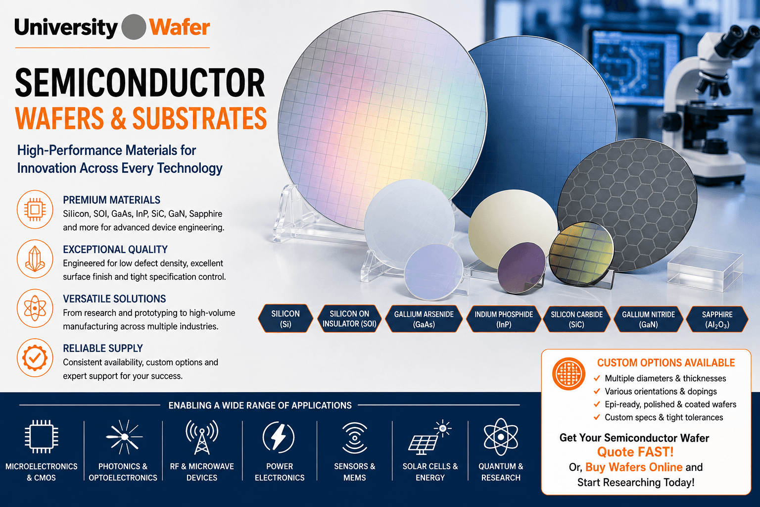
- Material: Si, SOI, GaAs, InP, SiC, GaN, sapphire, or another substrate
- Diameter: selected for equipment compatibility and process requirements
- Crystal orientation: such as (100), (111), (0001), or material-specific orientations
- Conductivity type: n-type, p-type, semi-insulating, or nominally undoped where applicable
- Dopant and resistivity: selected according to electrical requirements
- Thickness: including required tolerances
- Surface finish: SSP, DSP, epi-ready, or other application-specific preparation
- Wafer geometry: TTV, bow, warp, flats, notch, and edge profile when relevant
- Coatings or epitaxy: oxide, nitride, metals, or semiconductor epitaxial layers when required
Matching these specifications to the fabrication process can improve wafer handling, lithography, deposition, epitaxy, etching, metrology, and overall experimental repeatability.
Get Your Semiconductor Wafer Quote FAST!
Or, Buy Wafers Online
and Start Researching Today!
How Semiconductor Wafers Are Manufactured
Manufacturing a semiconductor wafer begins with producing high-purity crystalline material with carefully controlled electrical and structural properties. The exact growth method depends on the semiconductor. Silicon, for example, is commonly grown as a single-crystal ingot using the Czochralski (CZ) process or the float-zone (FZ) method.
After crystal growth, the ingot is oriented, shaped, and sliced into wafers. Subsequent processing can include edge grinding, lapping, etching, cleaning, and chemical mechanical polishing (CMP). The objective is to produce wafers with controlled thickness, surface roughness, total thickness variation (TTV), bow, warp, and crystallographic orientation.
Czochralski vs. Float-Zone Silicon Wafers
Czochralski silicon wafers are produced by pulling a rotating seed crystal from molten silicon contained in a silica crucible. CZ growth is the dominant method for producing large-diameter silicon crystals and allows controlled incorporation of dopants during crystal growth. Interaction with the silica crucible also introduces oxygen into the crystal, which can influence subsequent processing and material properties.
Float-zone (FZ) silicon is produced without a crucible. A localized molten zone travels through a high-purity silicon rod, allowing many impurities to segregate away from the growing crystal. FZ silicon can therefore achieve very low oxygen concentrations and very high resistivity, making high-resistivity silicon wafers useful for RF devices, detectors, power electronics, and specialized semiconductor research.
N-Type and P-Type Semiconductor Wafers
The electrical properties of many semiconductor substrates are intentionally modified through doping. In silicon, adding donor impurities such as phosphorus or arsenic can produce n-type silicon, in which electrons are the majority carriers. Acceptor dopants such as boron produce p-type silicon , in which holes are the majority carriers.
Dopant species and concentration affect carrier concentration, resistivity, mobility, junction behavior, and other electrical characteristics. Semiconductor wafers can therefore be ordered with specific conductivity types and resistivity ranges to support particular experiments or device structures.
Researchers studying these relationships can learn more about semiconductor doping and carrier mobility and how increasing ionized-impurity concentrations can affect electrical transport.
Semiconductor Crystal Orientation
Crystal orientation describes how the wafer surface is aligned relative to the crystal lattice. Orientation can influence surface atomic structure, oxidation, epitaxy, cleavage, etching behavior, and some electrical or mechanical properties.
For silicon, common surface orientations include (100) and (111). Silicon (100) is widely used in CMOS and many microfabrication processes, while silicon (111) is important in selected epitaxial, MEMS, surface-science, and anisotropic-etching applications.
Orientation is particularly important for anisotropic silicon etching . Etchants such as KOH and TMAH can etch different silicon crystal planes at substantially different rates, enabling crystallographically defined structures for MEMS and microfabrication.
Wafer Surface Finish: SSP, DSP and Epi-Ready
Surface finish should be selected according to the intended fabrication process. Single-side polished (SSP) wafers have one highly polished working surface, while double-side polished (DSP) wafers have polished surfaces on both sides.
DSP wafers can be advantageous for MEMS, optical processing, backside alignment, transmission measurements, wafer bonding, and processes requiring controlled surfaces on both sides. Epitaxial applications may require an epi-ready semiconductor wafer with tightly controlled surface roughness, cleanliness, crystallographic quality, and defect levels.
Chemical Mechanical Polishing of Semiconductor Wafers
Chemical mechanical polishing (CMP) combines chemical reactions with mechanical abrasion to produce highly planar semiconductor surfaces. CMP is widely used in wafer preparation and integrated-circuit fabrication where surface planarity is critical for subsequent lithography, deposition, bonding, or multilayer processing.
Surface roughness, scratches, particles, contamination, and subsurface damage can affect subsequent device processing. For this reason, semiconductor-grade polishing and cleaning are important when substrates will be used for epitaxy, thin-film deposition, wafer bonding, or high-resolution lithography.
Epitaxial Semiconductor Wafers
Epitaxy is the growth of a crystalline layer with a defined crystallographic relationship to the underlying substrate. The deposited layer may have a different doping concentration, composition, or electronic properties from the substrate, allowing engineers to create controlled semiconductor structures.
Silicon epitaxial wafers are used in numerous semiconductor applications, while compound semiconductor epitaxy can produce structures involving GaAs, InP, GaN, AlGaN, InGaAs, and related materials.
Depending on the material system, epitaxial layers may be grown using techniques such as chemical vapor deposition (CVD), metal-organic chemical vapor deposition (MOCVD), or molecular beam epitaxy (MBE) .
Thin Films and Dielectric Layers on Semiconductor Wafers
Semiconductor substrates are frequently supplied or processed with additional thin-film layers. Silicon wafers, for example, can be coated with thermal silicon dioxide (SiO₂), silicon nitride, metals, polymers, or deposited dielectric films.
Silicon dioxide is an electrically insulating material used in MOS structures, surface passivation, masking, optical structures, and many microfabrication processes. Silicon nitride can provide electrical insulation, diffusion barriers, passivation, mechanical membranes, and optical functionality depending on its composition and deposition process.
Semiconductor Wafers for MEMS
MEMS semiconductor wafers are used to fabricate microscopic mechanical structures integrated with electrical or optical functionality. Silicon is particularly important for MEMS because its mechanical properties, mature lithographic processing, and well-characterized anisotropic etching enable precise fabrication of beams, membranes, cavities, cantilevers, resonators, and sensors.
SOI wafers are especially useful for many MEMS processes because the silicon device layer can define structural thickness while the buried oxide can serve as an electrical insulator or sacrificial/etch-stop layer in appropriate fabrication schemes.
Semiconductor Wafers for Photonics and Optoelectronics
Semiconductor materials are also fundamental to photonic and optoelectronic technologies. Silicon and SOI are important platforms for integrated silicon photonics, while direct-bandgap III-V materials such as gallium arsenide (GaAs) and indium phosphide (InP) are widely used for efficient light emission and detection.
Applications include semiconductor lasers, LEDs, photodetectors, modulators, optical communication components, photovoltaic devices, and photonic integrated circuits. Material selection depends strongly on the wavelength range, band structure, lattice compatibility, carrier transport, and device architecture.
Wide-Bandgap Wafers for Power Electronics
Silicon carbide (SiC) and gallium nitride (GaN) are important wide-bandgap semiconductor materials. Their high critical electric fields enable device designs that can operate at higher electric fields than conventional silicon devices.
SiC is particularly important for high-voltage power MOSFETs and Schottky diodes, while GaN is widely used in high-frequency power conversion and RF electronics. The best material depends on voltage, frequency, thermal management, device topology, cost, and manufacturing requirements.
Wafer Diameter and Fabrication Equipment Compatibility
Semiconductor wafers are available in multiple diameters. Common research and production sizes include 2 inch, 3 inch, 4 inch (100mm), 6 inch (150mm), 8 inch (200mm), and 12 inch (300mm), although availability depends strongly on the substrate material.
Larger wafers provide more usable area per substrate and can increase the number of devices fabricated per wafer, but wafer diameter must match the capabilities of lithography, deposition, etching, cleaning, metrology, and handling equipment. Compound semiconductor materials are not necessarily available in the same maximum diameters as silicon.
How to Choose a Semiconductor Wafer
Choosing the correct semiconductor substrate begins with the requirements of the device or experiment. Important factors include electronic band structure, carrier transport, thermal properties, crystal quality, lattice compatibility, electrical resistivity, optical response, wafer geometry, and process compatibility.
Before requesting a quote, consider specifying:
- Material: Si, SOI, SiC, GaAs, InP, GaN, sapphire, or another substrate
- Wafer diameter and required dimensional tolerances
- Crystal orientation and off-axis angle when applicable
- Conductivity type: n-type, p-type, semi-insulating, or nominally undoped
- Dopant and target resistivity or carrier concentration
- Wafer thickness and total thickness variation (TTV)
- Surface finish: SSP, DSP, epi-ready, or another preparation
- Bow and warp requirements
- Surface coatings such as oxide, nitride, metals, or other thin films
- Epitaxial layers when required for the device structure
UniversityWafer supplies semiconductor substrates and research wafers for universities, laboratories, government research, industrial R&D, prototyping, and specialized semiconductor fabrication.
Related Semiconductor Wafers & Substrates
- Silicon Wafers – Explore silicon substrates by diameter, orientation, resistivity, doping, thickness, and surface finish.
- Silicon-on-Insulator (SOI) Wafers – Engineered silicon substrates with a buried oxide layer for MEMS, CMOS, RF, and silicon photonics research.
- III-V Semiconductor Wafers – Explore GaAs, InP, GaN, InAs, GaSb, and other III-V compound semiconductor materials.
- Indium Phosphide (InP) Wafers – III-V substrates for photonic integrated circuits, optical communications, high-speed electronics, and optoelectronic devices.
- Silicon Carbide (SiC) Wafers – Wide-bandgap semiconductor substrates for high-voltage, high-temperature, RF, and power-electronic device research.
- Gallium Nitride (GaN) Wafers – Wide-bandgap GaN materials for power electronics, RF devices, LEDs, lasers, and advanced optoelectronics.
- Sapphire Wafers & Al₂O₃ Substrates – Single-crystal sapphire substrates for GaN epitaxy, optics, RF, LEDs, and thin-film research.
- High-Resistivity Silicon Wafers – High-resistivity silicon substrates for RF, detectors, MEMS, power devices, and specialized research.
- Silicon Epitaxial Wafers – Learn about crystalline silicon epitaxial layers for semiconductor device fabrication and materials research.
- Semiconductor Band Gap – Understand how semiconductor band structure influences optical, electronic, and device properties.
- Chemical Mechanical Polishing (CMP) – Learn about semiconductor wafer planarization and surface preparation for advanced fabrication processes.