
What Are Prime Grade Silicon Wafers?
Prime grade silicon wafers are high-quality, single-crystal silicon substrates intended for demanding semiconductor, microfabrication, MEMS, photonics, sensor, and materials-research applications. Compared with lower-cost test or mechanical-grade wafers, prime wafers are generally supplied with tighter control of important parameters such as crystal orientation, resistivity, thickness, surface finish, flatness, and wafer geometry.
However, "prime grade" is not one universal material specification. Requirements vary with wafer manufacturer, diameter, application, and customer specification. Researchers should therefore select wafers using the actual electrical, crystallographic, dimensional, and surface parameters required by their process rather than relying on the grade designation alone.
Prime Silicon Wafer Specifications
Important specifications to consider when selecting a device-grade silicon wafer include:
- Wafer diameter: Select the diameter required by your fabrication equipment, sample geometry, or research process.
- Crystal growth method: Czochralski (CZ) and Float Zone (FZ) silicon have different impurity profiles and available resistivity ranges.
- Conductivity type: Silicon may be supplied as p-type, n-type, or high-resistivity material depending on the application.
- Dopant: Common dopants include boron for p-type silicon and phosphorus, arsenic, or antimony for n-type silicon.
- Resistivity: Resistivity is related to dopant concentration and carrier mobility and is an important parameter for electronic, RF, detector, MEMS, and other device applications.
- Crystal orientation: Common surface orientations include Si(100), Si(111), and Si(110). Orientation can influence oxidation, etching, epitaxy, surface structure, and device processing.
- Thickness: Standard thickness depends strongly on wafer diameter and applicable manufacturing standards. Custom thin or thick silicon may require additional processing.
- Surface finish: Prime wafers may be supplied single-side polished (SSP) or double-side polished (DSP), depending on the process requirements.
- Wafer geometry: Parameters such as total thickness variation (TTV), bow, warp, edge profile, and flatness can become important in lithography, bonding, MEMS, and wafer-level processing.
CZ vs. Float Zone Prime Silicon
Prime-grade silicon can be produced using different crystal-growth techniques. Two important methods are Czochralski (CZ) and Float Zone (FZ) crystal growth.
Czochralski (CZ) Silicon
In the Czochralski process, a seed crystal is pulled from molten silicon contained in a silica crucible. CZ growth is widely used for commercial silicon wafer production and can produce large-diameter, high-quality single-crystal silicon.
Because the molten silicon contacts a silica crucible, CZ silicon normally contains a measurable concentration of oxygen. Oxygen is not necessarily undesirable: depending on the device process, it can influence mechanical strength, thermal processing, precipitation, and internal gettering behavior.
Float Zone (FZ) Silicon
In the Float Zone process, a localized molten zone is passed through a silicon rod without using a crucible to contain the melt. This allows very low oxygen and carbon contamination compared with conventional CZ silicon and enables high-purity, high-resistivity material.
High-resistivity silicon wafers are often selected for RF, microwave, detector, photonic, and specialized electronic research where reduced free-carrier conduction or low substrate loss is important.
P-Type and N-Type Prime Silicon Wafers
The electrical properties of silicon can be intentionally controlled by introducing small concentrations of dopant atoms into the crystal.
P-type silicon is commonly produced using acceptor dopants such as boron. These acceptors increase the hole concentration, making holes the majority carriers.
N-type silicon is produced using donor dopants such as phosphorus, arsenic, or antimony. These donors increase the electron concentration, making electrons the majority carriers.
Neither conductivity type is universally "better." The appropriate dopant, conductivity type, and silicon resistivity depend on the intended device structure and fabrication process.
Prime Silicon Wafer Crystal Orientations
Silicon wafers are cut so that their polished surface has a defined orientation relative to the single-crystal lattice. Common orientations include:
- Si(100): Widely used in CMOS processing, MOS structures, MEMS, oxidation studies, and general semiconductor research.
- Si(111): Important for selected epitaxial systems, surface-science experiments, thin-film growth, and processes where the (111) surface symmetry is advantageous.
- Si(110): Used in specialized electronic, MEMS, anisotropic-etching, and crystallographic applications.
Orientation is especially important in anisotropic wet etching because crystallographic planes can etch at very different rates in solutions such as KOH or TMAH. Researchers should therefore select orientation according to the actual fabrication process rather than treating all silicon surfaces as equivalent.
Learn more about silicon wafer orientation .
SSP vs. DSP Prime Silicon Wafers
Single-side polished (SSP) silicon has one polished device surface, while the backside is not polished to the same device-grade finish. SSP wafers are suitable for many conventional semiconductor, deposition, lithography, and materials-research processes.
Double-side polished (DSP) silicon provides polished surfaces on both sides. DSP wafers can be advantageous for wafer bonding, MEMS, backside lithography, optical transmission experiments, thin-wafer processing, and processes requiring controlled surfaces on both sides.
Prime Grade vs. Test and Mechanical Silicon Wafers
Different silicon wafer grades serve different purposes. A prime-grade wafer is generally selected when substrate quality and tighter specifications are important to the experiment or device process.
Lower-cost test, monitor, or mechanical-grade wafers can be useful for equipment setup, process development, coating trials, handling tests, furnace loading, deposition qualification, and other work where full device-grade specifications are unnecessary.
Using prime wafers for every experiment may add unnecessary cost, while using lower-grade material for a process that depends on tight crystallographic, electrical, surface, or dimensional specifications can introduce unwanted variability.
Prime Silicon Wafer Applications
Prime-grade silicon substrates are used in research and fabrication involving:
- Semiconductor device fabrication
- Photolithography and microfabrication
- Thin-film deposition
- Thermal oxidation and dielectric research
- MEMS and microsensors
- Microelectronics
- Photonics and silicon photonics
- RF and microwave research
- Wafer bonding
- Epitaxial and thin-film growth
- Surface science and materials characterization
- University and laboratory process development
How to Specify a Prime Silicon Wafer
For the fastest and most accurate quote, provide as many of the following specifications as possible:
- Diameter
- CZ or FZ growth method
- P-type, n-type, or nominally undoped/high-resistivity
- Dopant
- Resistivity range (Ω·cm)
- Crystal orientation
- Thickness and tolerance
- SSP or DSP
- Surface roughness, when required
- TTV, bow, and warp limits, when important
- Quantity
- Intended application or fabrication process
Get Your Prime Grade Silicon Wafer Quote FAST! Or Buy Wafers Online and start researching today!
Prime Grade Silicon Wafers for Semiconductor Fabrication
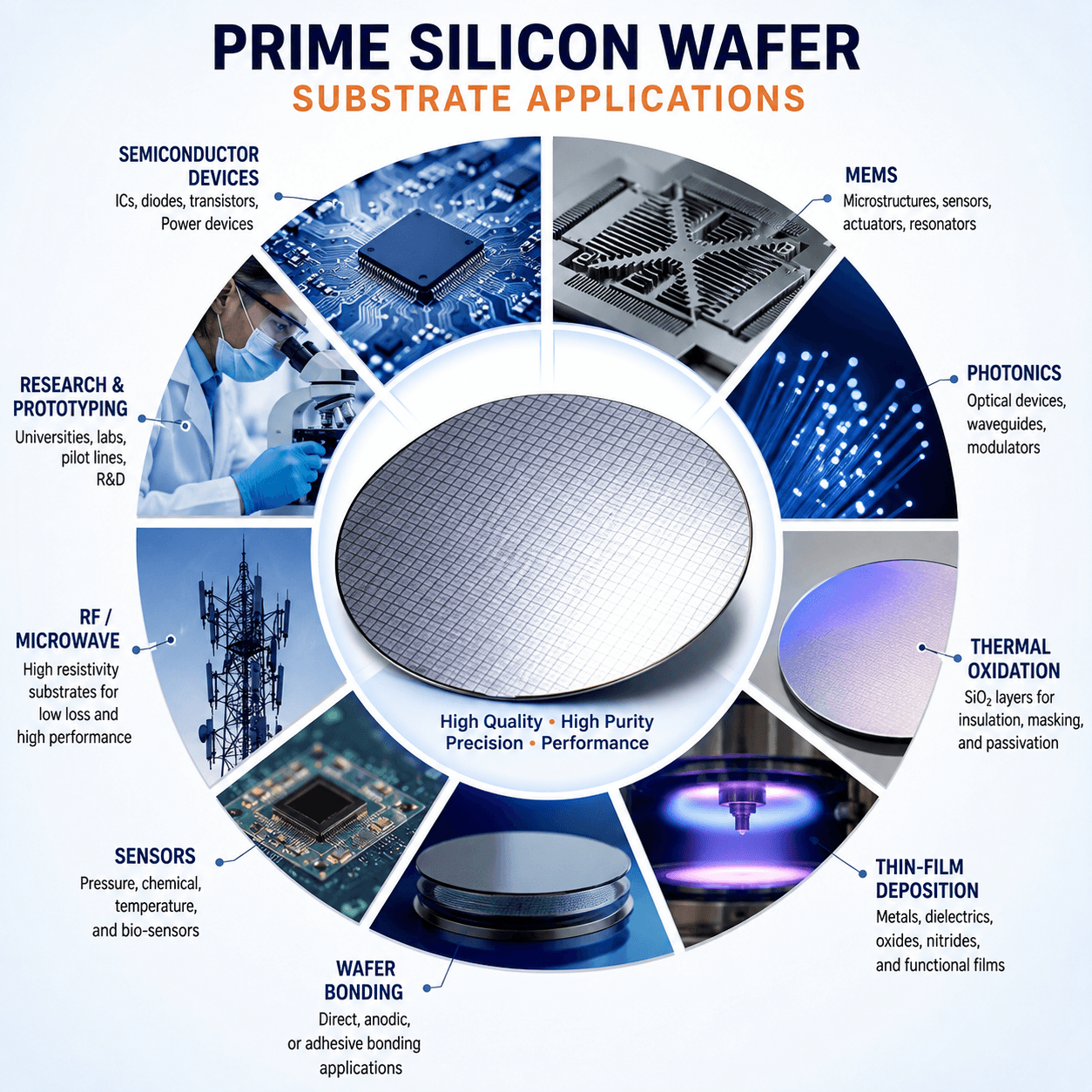
Prime grade silicon wafers provide high-quality, single-crystal substrates for processes in which surface condition, crystallographic orientation, electrical properties, and wafer geometry can influence fabrication results. They are commonly selected for semiconductor devices, MEMS, photonics, sensors, thin-film research, lithography, oxidation, and other precision microfabrication processes.
The appropriate wafer is determined by the process rather than by the word prime alone. Diameter, crystal growth method, conductivity type, dopant, resistivity, orientation, thickness, surface finish, and dimensional tolerances should all be considered when specifying a device-grade silicon substrate.
Why Surface Quality Matters
Many semiconductor processes begin directly on the polished silicon surface. Surface roughness, particles, scratches, contamination, and crystallographic damage can therefore affect subsequent processing. Prime wafers are typically selected when a high-quality polished surface is required for device fabrication or controlled research.
A properly prepared silicon surface can support processes such as photolithography, thin-film deposition, thermal oxidation, wafer bonding, surface characterization, and selected epitaxial processes.
The required surface specification depends on the application. For example, a wafer intended for optical bonding or precision metrology may require different roughness, flatness, and cleanliness specifications than a substrate used for a preliminary deposition experiment.
Prime Silicon Wafers for Photolithography
Prime silicon wafers are frequently used as starting substrates for photolithography and microfabrication. A smooth, controlled surface supports photoresist coating, exposure, development, pattern transfer, etching, deposition, and lift-off processes.
Wafer flatness and local geometry become increasingly important as feature sizes decrease or when lithography equipment requires accurate focusing across the wafer surface. Parameters such as total thickness variation (TTV), bow, and warp may therefore be important in precision processes.
Prime Silicon for Thermal Oxidation
Silicon can be thermally oxidized to form a layer of silicon dioxide (SiO2). Thermal oxide is used in semiconductor research as an electrical insulator, surface passivation layer, masking material, optical layer, and dielectric in selected device structures.
Oxide growth rate and resulting film properties depend on factors including temperature, oxidizing ambient, process time, crystal orientation, wafer condition, and doping level.
UniversityWafer can also supply thermal oxide silicon wafers for researchers who require silicon substrates with an existing SiO2 layer.
Thin-Film Deposition on Prime Silicon
Prime-grade silicon provides a well-characterized substrate for thin-film deposition and materials research. Depending on the experiment, deposited materials may include metals, dielectrics, semiconductors, oxides, nitrides, polymers, and other functional thin films.
Common deposition techniques include physical vapor deposition (PVD), chemical vapor deposition (CVD), atomic layer deposition (ALD), evaporation, and sputtering. Substrate preparation, surface chemistry, temperature, film stress, and thermal-expansion mismatch can influence adhesion and film quality.
Prime Silicon Wafers for MEMS
MEMS fabrication often uses single-crystal silicon because its mechanical, electrical, and crystallographic properties are well characterized and compatible with established microfabrication techniques.
Prime silicon can be used to fabricate structures such as membranes, cantilevers, beams, cavities, microchannels, sensors, and actuators. Crystal orientation is particularly important when anisotropic wet etching is used because different silicon crystal planes can exhibit substantially different etch rates.
For processes requiring electrical or mechanical isolation between a thin device layer and the underlying substrate, silicon-on-insulator (SOI) wafers may be more appropriate than conventional bulk silicon.
Prime Silicon for Sensors and Microelectronics
Controlled doping and mature silicon processing make prime silicon suitable for a broad range of electronic and sensor research. Applications can include test structures, diodes, transistors, resistive devices, capacitive structures, chemical sensors, pressure sensors, temperature sensors, and other microsystems.
Electrical behavior depends strongly on the wafer's conductivity type, dopant concentration, resistivity, carrier mobility, temperature, and device geometry. Researchers should therefore specify electrical properties according to the intended device rather than selecting a wafer solely by diameter or surface finish.
High-Resistivity Silicon for RF and Photonics
High-resistivity silicon is useful when reduced free-carrier conduction or lower substrate-related electrical loss is desired. Depending on the complete material specification and device design, these substrates can be useful for RF, microwave, detector, photonic, and specialized sensor research.
Float Zone silicon is frequently associated with high-resistivity applications because the crucible-free growth process enables low oxygen contamination and high material purity. However, the correct substrate should be chosen according to the required resistivity, impurity concentration, diameter, device structure, and processing conditions.
Prime Silicon for Wafer Bonding
Prime and double-side polished silicon wafers can be useful for wafer bonding because bonding processes can be sensitive to surface roughness, cleanliness, particles, bow, warp, and flatness.
Depending on the materials and process, bonding approaches may include direct bonding, anodic bonding, adhesive bonding, eutectic bonding, or other intermediate-layer techniques. Not every bonding method uses the same surface preparation or wafer specification.
Prime Grade vs. Epitaxial Silicon Wafers
A prime-grade silicon wafer and an epitaxial silicon wafer are not synonymous.
A conventional prime wafer is a high-quality bulk single-crystal silicon substrate. An epitaxial wafer contains a crystalline silicon layer grown on a crystalline substrate. The epitaxial layer can be engineered with electrical properties different from those of the underlying wafer, including controlled thickness and doping.
Researchers requiring a specific device-layer structure should therefore determine whether a polished bulk prime wafer is sufficient or whether an epitaxial layer is necessary.
Prime Grade vs. SOI Silicon Wafers
Conventional prime silicon is also different from silicon-on-insulator (SOI). An SOI wafer typically contains a crystalline silicon device layer separated from the handle substrate by a buried insulating layer, commonly silicon dioxide.
SOI is particularly useful for applications requiring a controlled thin silicon device layer, electrical isolation, reduced parasitic capacitance, or specialized MEMS structures. Bulk prime silicon remains the simpler and often more economical choice when those features are unnecessary.
Prime, Test, Monitor, and Reclaimed Silicon
Selecting the appropriate wafer grade can reduce research costs while maintaining the specifications required by the process.
| Wafer Type | Typical Purpose | When to Consider It |
|---|---|---|
| Prime Grade | Device fabrication and precision research | When electrical, crystallographic, surface, and dimensional specifications are important |
| Test Grade | Process development and laboratory testing | When full prime-grade specifications are not required |
| Monitor Wafer | Process and equipment monitoring | For deposition, oxidation, furnace, etch, or equipment qualification processes |
| Reclaimed Wafer | Selected non-device and process-development applications | When previously processed silicon can be stripped, polished, cleaned, and reused within the requirements of the application |
These categories should be treated as general descriptions rather than universal standards. The actual wafer specification should always be reviewed before determining whether a particular grade is suitable for a fabrication process.
Common Prime Silicon Wafer Applications
| Application | Important Wafer Considerations |
|---|---|
| Semiconductor Devices | Dopant, resistivity, orientation, surface quality |
| Photolithography | Flatness, surface quality, TTV, cleanliness |
| MEMS | Orientation, thickness, TTV, bow, warp |
| RF / Microwave | Resistivity, impurity concentration, substrate loss |
| Photonics | Resistivity, orientation, surface quality, device structure |
| Wafer Bonding | Surface roughness, flatness, particles, bow and warp |
| Thin-Film Research | Surface condition, orientation, thermal compatibility |
| Thermal Oxidation | Orientation, doping, surface condition, thermal process |
Choosing the Right Prime Grade Silicon Wafer
There is no single prime silicon specification that is ideal for every experiment. A semiconductor device researcher may prioritize dopant and resistivity, while a MEMS researcher may care more about orientation, thickness, TTV, and mechanical geometry. A wafer-bonding project may place greater emphasis on surface roughness, flatness, bow, and cleanliness.
When requesting a quote, include your intended application whenever possible. Knowing whether the substrate will be used for lithography, oxidation, deposition, bonding, MEMS, RF, photonics, or another process can help identify the most appropriate prime grade silicon wafer specification.
Buy Prime Grade Silicon Wafers
UniversityWafer supplies prime silicon wafers for universities, laboratories, semiconductor research, microfabrication, MEMS, photonics, sensors, thin-film processing, and device development. Custom specifications may be available for diameter, crystal growth method, conductivity type, dopant, resistivity, orientation, thickness, and surface finish.