
Accelerate Your Aerospace Semiconductor Research
Bring your hybrid-electric aircraft, electric propulsion, MEMS sensor, and wide-bandgap semiconductor concepts to life with precision-engineered silicon substrates from UniversityWafer, Inc. Researchers can order small quantities, evaluate advanced thin-film coatings, and optimize device performance for next-generation aerospace electronics, avionics, thermal-management systems, and aircraft control technologies.
Get Your Aerospace Wafer Quote FAST! Or, Buy Online and Start Researching Today!
Silicon Substrates for Aerospace Prototyping
Researchers and engineers working on hybrid-electric propulsion, electric aircraft power systems, MEMS sensors, SiC power electronics, and high-temperature semiconductor devices rely on UniversityWafer for precision substrates that support every stage of development—from material evaluation and wafer processing to prototype fabrication and reliability testing.
Available options include silicon wafers with custom crystal orientation, dopant type, resistivity, thickness, surface finish, and dielectric coatings. These specifications can be selected for aerospace MEMS, control electronics, thermal testing, wafer bonding, heterogeneous integration, and semiconductor process development.
- Request a Custom Quote for silicon wafers, SOI substrates, SiC wafers, and specialty materials.
- Browse Silicon Substrates in stock or request custom wafer specifications.
- Contact Technical Support to discuss doping, crystal orientation, resistivity, wafer thickness, polishing, and oxide or nitride coatings.
Recommended Wafer Materials for Aerospace Research
- Silicon Wafers – for MEMS fabrication, CMOS control electronics, sensors, wafer bonding, and semiconductor process development.
- Silicon Carbide (SiC) Wafers – for high-voltage power conversion, electric propulsion drives, inverters, and high-temperature electronics.
- Silicon-on-Insulator (SOI) Wafers – for MEMS devices, dielectric isolation, low-leakage circuits, radiation-tolerant electronics, and high-temperature sensors.
- Thermal Oxide Wafers – for dielectric isolation, passivation, thermal testing, device fabrication, and wafer-level integration.
- Silicon Nitride Wafers – for MEMS membranes, etch masks, passivation layers, sensors, and high-temperature wafer processing.
- Quartz Substrates – for optical, thermal, RF, microwave, and sensor-development applications.
Common Aerospace Wafer Specifications
Aerospace research projects often require tightly controlled wafer specifications to support electrical performance, mechanical stability, and repeatable fabrication. Frequently requested options include:
- Wafer diameter: Small research wafers through 300 mm substrates.
- Crystal orientation: <100>, <110>, or <111> silicon.
- Dopant type: P-type or N-type material.
- Resistivity: Low-, medium-, or high-resistivity silicon.
- Surface finish: Single-side polished, double-side polished, etched, lapped, or as-cut.
- Thin-film coatings: Thermal oxide, silicon nitride, metals, and custom deposited layers.
- Wafer thickness: Standard or custom thickness for stiffness, vibration tolerance, and through-wafer processing.
Support for MEMS and Aerospace Sensor Development
Silicon and SOI wafers provide established platforms for manufacturing MEMS accelerometers, gyroscopes, pressure sensors, temperature sensors, strain gauges, and inertial measurement devices. These components are used in flight-control systems, structural-health monitoring, navigation, engine monitoring, unmanned aerial vehicles, satellites, and spacecraft.
Double-side polished silicon wafers are especially useful for backside lithography, through-wafer etching, optical alignment, wafer bonding, and suspended MEMS structures. Thermal oxide and silicon nitride coatings can add electrical isolation, surface passivation, etch resistance, and process flexibility.
Materials for SiC and GaN Power Electronics
Electric aircraft and hybrid-electric propulsion systems increasingly rely on silicon carbide and gallium nitride power devices for efficient switching and high-power operation. Silicon substrates complement these wide-bandgap semiconductors by supporting control circuits, gate drivers, monitoring electronics, temperature sensors, and multi-material integration experiments.
Researchers can use UniversityWafer substrates to evaluate SiC-on-silicon structures, wafer bonding, thermal expansion mismatch, interconnect reliability, thin-film adhesion, and thermal cycling performance before full device integration.
Fast Turnaround for Aerospace Research Projects
UniversityWafer supports universities, aerospace laboratories, engineering teams, and startups by offering low minimum order quantities, small research lots, and worldwide delivery. Whether you are testing SiC-on-Si structures, MEMS accelerometers, SOI sensors, thermal coatings, or heterogeneous semiconductor assemblies, our substrates help you move from concept to prototype more efficiently.
Precision Wafers for Advanced Aerospace Applications
UniversityWafer supplies wafers and substrates for aerospace electronics, electric propulsion research, MEMS fabrication, thermal-management studies, RF devices, photonics, sensors, and advanced semiconductor integration. Our broad range of materials and custom specifications helps researchers select a reliable substrate for demanding laboratory and prototype applications.
Silicon Substrates for Aerospace Electronics and Efficient Aircraft Systems
Aerospace innovation increasingly depends on lighter, more efficient, and thermally robust electronic systems. As manufacturers develop hybrid-electric aircraft, fully electric aircraft, unmanned aerial vehicles, and advanced spacecraft, research teams require precision semiconductor materials that can perform reliably under high temperatures, vibration, radiation, and repeated thermal cycling.
Recent developments in silicon carbide (SiC) power electronics have demonstrated major improvements in power density, switching efficiency, and system weight for electric aircraft propulsion. These benefits make SiC and gallium nitride (GaN) important wide-bandgap semiconductor materials for aerospace power conversion. Silicon substrates, however, remain essential for the sensors, control electronics, test structures, gate drivers, and monitoring circuits used throughout aerospace research and development.
Why Silicon Substrates Remain Essential in Aerospace Research
Although SiC and GaN receive significant attention for high-voltage and high-frequency systems, silicon substrates remain indispensable for signal processing, thermal monitoring, power management, control electronics, and sensor fabrication. Aerospace engineers rely on silicon's mechanical stability, electrical uniformity, crystalline quality, and compatibility with established semiconductor fabrication processes.
Silicon wafers can support CMOS circuits, MEMS structures, oxide and nitride coatings, thin-film deposition, photolithography, and wafer-level integration. This versatility makes silicon suitable for early-stage prototypes as well as the development of integrated aerospace electronics.
- Thermal management research: Silicon wafers help researchers evaluate heat dissipation, thermal interface materials, wafer bonding, and package reliability in high-temperature environments.
- Control and sensing: MEMS and CMOS devices fabricated on silicon can measure vibration, acceleration, pressure, temperature, and mechanical strain within aircraft systems.
- System reliability: Precision silicon substrates provide consistent mechanical and electrical properties for aerospace prototypes exposed to shock, vibration, and repeated thermal cycling.
- Semiconductor process development: Silicon wafers are used for thin-film deposition, lithography, etching, device testing, and multi-material wafer integration.
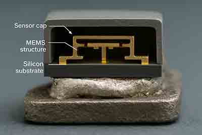
Supporting Wide-Bandgap Semiconductor Power Electronics
The next generation of electric aircraft propulsion depends on integrating SiC power modules and GaN power devices with silicon-based control and protection electronics. Wide-bandgap semiconductors can operate at higher voltages, temperatures, and switching frequencies than conventional silicon power devices, helping reduce the size and weight of power converters, inverters, and motor drives.
Within these hybrid semiconductor systems, silicon substrates can be used to fabricate gate drivers, monitoring circuits, control ICs, temperature sensors, current sensors, and protection structures that help SiC and GaN devices operate efficiently and safely.
Researchers use silicon wafers for:
- Testing wafer bonding and interface strength between silicon, SiC, metals, ceramics, and dielectric layers.
- Developing SiC-on-silicon test structures and multi-material semiconductor assemblies.
- Evaluating thermal expansion mismatch and mechanical stress during temperature cycling.
- Benchmarking thermal conductivity, heat spreading, and junction-temperature performance.
- Prototyping gate-driver circuits and power-management electronics for electric propulsion systems.
UniversityWafer's selection of silicon substrates allows aerospace research groups to specify wafer diameter, thickness, crystal orientation, dopant type, resistivity, and surface finish. These parameters influence electrical conductivity, mechanical stiffness, etching behavior, device isolation, and compatibility with downstream wafer-processing steps.
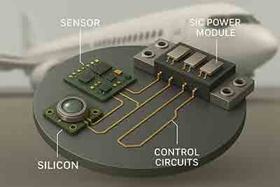
Silicon Wafers for Aerospace MEMS Sensors
Beyond propulsion, modern aircraft and spacecraft rely on networks of microelectromechanical systems (MEMS) to measure pressure, acceleration, vibration, angular motion, temperature, and structural strain. Silicon's low defect density, high mechanical stiffness, predictable etching characteristics, and compatibility with silicon dioxide and silicon nitride make it a preferred substrate for miniature aerospace sensors.
UniversityWafer supplies single-side polished and double-side polished silicon wafers for MEMS fabrication. Double-side polished wafers are particularly useful for optical alignment, through-wafer processing, backside lithography, wafer bonding, and the fabrication of suspended membranes or proof-mass structures.
Optional thermal oxide and silicon nitride coatings can provide dielectric isolation, passivation, masking layers, and surface protection during MEMS wafer processing.
These substrates support the development of:
- MEMS accelerometers for inertial navigation and flight-control systems.
- Gyroscopes and inertial measurement units.
- Pressure sensors for altitude, airflow, and propulsion monitoring.
- Temperature sensors for batteries, motors, inverters, and power modules.
- Micro-vibration and shock sensors for structural-health monitoring.
- Strain gauges and resonant sensors for aircraft components.
- Microfluidic devices for aerospace fuel, cooling, and environmental testing.
By supporting both MEMS sensor research and wide-bandgap semiconductor integration, UniversityWafer helps bridge the gap between laboratory prototypes and field-ready aerospace electronics.
Thermal Management and High-Temperature Testing
Thermal management is a critical challenge in electric propulsion, avionics, radar, battery systems, and high-power aerospace electronics. Excessive heat can reduce semiconductor efficiency, accelerate material degradation, and shorten device life.
Silicon wafers provide controlled surfaces for testing thin-film coatings, thermal interface materials, metallization, dielectric layers, and bonded semiconductor structures. Researchers can use them to evaluate:
- Heat spreading and thermal resistance.
- Thermal cycling and thermal shock.
- Wafer bow and residual film stress.
- Adhesion between deposited layers.
- Coefficient-of-thermal-expansion mismatch.
- High-temperature sensor stability.
- Package and interconnect reliability.
Silicon Wafer Specifications for Aerospace Applications
UniversityWafer offers silicon wafers in diameters from approximately 25 mm to 300 mm, with options for P-type or N-type doping, custom thickness, resistivity, crystal orientation, and surface finish. The appropriate specification depends on the device architecture, fabrication process, and operating environment.
- Crystal orientation: <100> silicon is widely used for CMOS and MEMS processing, while <111> silicon may be selected for specialized mechanical, etching, or sensor applications.
- Dopant type: Boron-doped P-type and phosphorus-, arsenic-, or antimony-doped N-type wafers are available for different electrical requirements.
- Resistivity: Low-, medium-, and high-resistivity silicon can support power electronics, control circuits, RF research, detectors, and electrically isolated test structures.
- Wafer thickness: Thickness can be selected according to mechanical stiffness, device handling, through-wafer etching, vibration tolerance, or bonding requirements.
- Surface finish: Single-side polished, double-side polished, etched, lapped, or as-cut surfaces may be selected for different research processes.
- Thin-film coatings: Thermal oxide, silicon nitride, metals, and other deposited layers can support dielectric isolation, passivation, etch masking, and thermal testing.
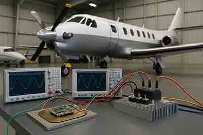
Silicon-on-Insulator Wafers for Aerospace Electronics
Silicon-on-insulator (SOI) wafers can provide additional electrical isolation, reduced parasitic capacitance, lower leakage current, and improved high-temperature performance. These properties make SOI substrates useful for aerospace MEMS sensors, radiation-tolerant electronics, RF systems, control circuits, and devices intended for harsh environments.
The buried oxide layer in an SOI wafer can also support suspended MEMS structures, thermal isolation, pressure-sensor membranes, and microfabricated devices requiring precisely controlled silicon device layers.
Applications of Silicon Substrates in Aerospace Research
- Hybrid-electric and fully electric aircraft propulsion
- Power converters and inverter control electronics
- SiC and GaN power-module integration
- MEMS accelerometers and gyroscopes
- Pressure, temperature, vibration, and strain sensors
- Inertial navigation systems
- Structural-health monitoring
- Thermal management and heat-spreader research
- High-temperature semiconductor testing
- Radiation-tolerant electronics research
- RF and microwave aerospace electronics
- Wafer bonding and heterogeneous integration
- Thin-film deposition and semiconductor process development
- Satellite, spacecraft, and unmanned aerial vehicle systems
Future of Semiconductor Materials in Electric Aircraft
The aerospace sector is rapidly adopting electric propulsion, autonomous flight systems, advanced sensors, and higher-power electronic architectures. These technologies require multi-material semiconductor integration involving silicon, silicon carbide, gallium nitride, SOI, dielectric coatings, metals, and thermal-management materials.
As aerospace electronics become more integrated, silicon will continue to provide an established platform for control circuits, MEMS sensors, wafer-level packaging, photonic components, and thermal test structures. SiC and GaN will complement silicon in the high-voltage and high-frequency portions of the system.
UniversityWafer supports this research by supplying small quantities for initial testing as well as custom wafer specifications for prototype development. From laboratory experiments to advanced aircraft systems, UniversityWafer silicon substrates help researchers develop safer, lighter, and more energy-efficient aerospace technologies.
Reference
Sinha, Sujita. November 4, 2025. New silicon-powered electric motor cuts hybrid plane weight, helps them fly farther. Interesting Engineering. Read the article .
Related Aerospace & Semiconductor Resources
- Silicon Substrates – Prime, test, and custom silicon substrates for aerospace electronics, MEMS, and semiconductor fabrication.
- Silicon Wafers – Research-grade silicon wafers available in multiple diameters, orientations, and resistivities.
- Silicon-on-Insulator (SOI) Wafers – Low-leakage substrates for MEMS devices, RF electronics, aerospace sensors, and harsh-environment applications.
- Silicon Carbide (SiC) Wafers – Wide-bandgap semiconductor substrates for power electronics, electric aircraft propulsion, and high-temperature devices.
- Gallium Nitride (GaN) Wafers – GaN substrates for RF amplifiers, radar systems, satellite communications, and high-frequency electronics.
- MEMS Applications – Silicon and SOI wafers for accelerometers, gyroscopes, pressure sensors, and inertial navigation systems.
- Thermal Oxide Wafers – Silicon substrates with precision SiO₂ layers for dielectric isolation, thermal management, and semiconductor processing.
- Silicon Nitride Wafers – LPCVD and PECVD silicon nitride coatings for MEMS fabrication, passivation, and dielectric isolation.
- Silicon Wafer Processing – Custom polishing, oxidation, wafer thinning, dicing, and thin-film deposition services for research and prototype development.
- Semiconductor Materials – Compare silicon, SiC, GaAs, GaN, germanium, and other materials used in advanced electronic devices.
- Photonic Devices – Semiconductor substrates for integrated photonics, optical communications, and aerospace sensing technologies.
- Research Substrates – Browse silicon, SOI, sapphire, SiC, GaN, quartz, fused silica, and other specialty substrates for university and industrial R&D.