
What Is Anisotropic Silicon Etching?
Anisotropic etching is a semiconductor fabrication process in which silicon is removed at different rates depending on its crystallographic direction. Unlike isotropic etching, which removes material approximately equally in all directions, anisotropic etching takes advantage of the crystal structure of silicon to create precisely defined features.
This orientation-dependent behavior makes anisotropic wet etching particularly useful for MEMS, silicon micromachining, sensors, microfluidics, V-grooves, cavities, and other three-dimensional microstructures.
Why Silicon Crystal Orientation Matters
The crystal orientation of a silicon wafer has a major influence on the geometry produced during anisotropic etching. Common orientations include (100), (110), and (111), with each exposing different crystallographic planes during the etching process.
For many applications, silicon wafers with a (100) orientation are commonly selected because anisotropic etching can produce well-defined structures bounded by slowly etching {111} planes.
(100) Silicon Wafers
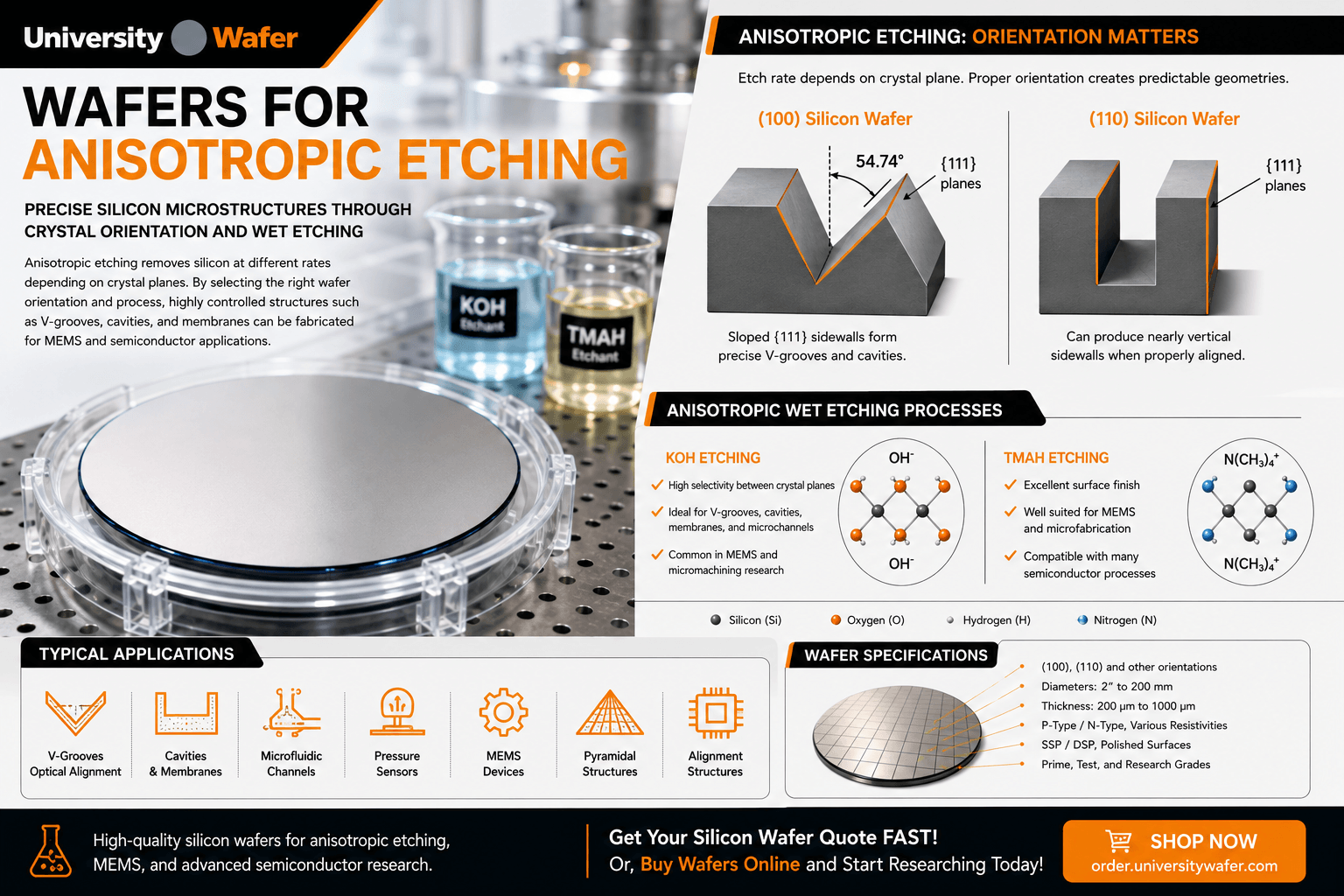
(100) silicon is widely used for anisotropic wet etching and MEMS fabrication. When properly aligned mask openings are etched using suitable anisotropic solutions, the slower-etching {111} planes can form characteristic sloped sidewalls.
In ideal crystallographic geometry, the angle between the (100) surface and {111} planes is approximately 54.74°. This predictable geometry is valuable when fabricating V-grooves, pyramidal structures, cavities, membranes, and other precisely defined features.
(110) Silicon Wafers
(110) silicon wafers can be useful when device designs require different crystallographic geometries. Proper mask alignment can expose {111} planes that form nearly vertical sidewalls relative to the wafer surface, making this orientation useful for specialized micromachining structures.
KOH Anisotropic Etching
Potassium hydroxide (KOH) is widely used for anisotropic wet etching of crystalline silicon. The etch rate varies significantly among silicon crystal planes, enabling researchers to create structures whose final geometry is strongly influenced by wafer orientation and mask alignment.
KOH etching is commonly investigated for the fabrication of:
- V-grooves and channels
- MEMS cavities
- Silicon membranes
- Microfluidic structures
- Pressure sensor structures
- Optical alignment features
- Pyramidal structures
- Bulk silicon micromachining
TMAH Silicon Etching
Tetramethylammonium hydroxide (TMAH) is another commonly used anisotropic silicon etchant. Like KOH, TMAH exhibits crystallographic selectivity and can be used to produce controlled microstructures on appropriately oriented silicon substrates.
TMAH is particularly useful in semiconductor process flows where compatibility with surrounding materials and fabrication requirements makes it preferable to other alkaline etchants.
Selecting Wafers for Anisotropic Etching
Selecting an appropriate wafer requires more than choosing its diameter. Researchers should consider the crystal orientation, orientation accuracy, wafer thickness, resistivity, conductivity type, surface finish, and dimensional tolerances required by the fabrication process.
Important wafer specifications may include:
- (100), (110), or other required crystal orientation
- Orientation accuracy and miscut
- Wafer diameter and thickness
- P-type or N-type conductivity
- Resistivity range
- Single-side or double-side polished surfaces
- Total thickness variation (TTV)
- Prime, test, or research-grade material
Get Your Silicon Wafer Quote FAST!
Or, Buy Wafers Online and Start Researching Today!
How Anisotropic Etching Creates Precise Microstructures
The geometry produced during anisotropic silicon etching is determined by the relationship between the wafer surface, crystallographic planes, mask orientation, etchant chemistry, temperature, and processing time. Because some silicon planes etch much more slowly than others, the crystal itself can help define the final shape of a microstructure.
This predictable behavior allows researchers to fabricate features with controlled dimensions and sidewall geometries without relying entirely on complex dry-etching equipment.
Common Structures Made with Anisotropic Etching
Anisotropic wet etching is especially valuable for creating three-dimensional structures directly within crystalline silicon. Depending on the silicon wafer orientation and mask geometry, researchers can fabricate a variety of microscopic features.
- V-grooves – Used for optical fiber alignment and precision positioning.
- Cavities – Useful for pressure sensors, MEMS devices, and suspended structures.
- Membranes – Thin silicon regions used in sensors and microsystems.
- Microchannels – Used in microfluidic and lab-on-chip research.
- Pyramidal structures – Used in optical, photovoltaic, and surface-engineering research.
- Alignment structures – Precisely etched features for photonic and microelectronic assembly.
Anisotropic Etching for MEMS Fabrication
MEMS fabrication is one of the most important applications for anisotropic silicon etching. Bulk micromachining can selectively remove portions of a silicon substrate to create mechanical structures while leaving other areas protected by an etch-resistant mask.
This approach can be used to fabricate components for pressure sensors, accelerometers, microfluidic devices, optical MEMS, resonators, and other microsystems.
Silicon substrates may also be combined with silicon nitride or silicon dioxide layers that can serve as masking, insulating, structural, or passivation materials during microfabrication.
Wet Etching vs. Dry Etching
Both wet and dry etching techniques are widely used in semiconductor fabrication, but they remove material through different mechanisms. Anisotropic wet etching uses chemical solutions and the crystallographic properties of silicon, while dry etching typically uses plasma-based processes to remove material.
| Characteristic | Anisotropic Wet Etching | Dry Etching |
|---|---|---|
| Process | Liquid chemical etchant | Plasma or reactive gas |
| Common Processes | KOH, TMAH | RIE, DRIE |
| Geometry Control | Strongly influenced by crystal orientation | Primarily controlled by process and mask geometry |
| Typical Structures | V-grooves, cavities, membranes | Trenches, holes, high-aspect-ratio features |
| Equipment | Relatively simple wet-processing equipment | Specialized vacuum and plasma equipment |
Masking Materials for Silicon Etching
Before anisotropic etching, selected areas of the wafer are typically protected with an etch-resistant masking layer. The mask defines where the silicon will be exposed to the chemical solution and therefore strongly influences the final structure.
Common masking materials can include silicon dioxide (SiO2) and silicon nitride (Si3N4). Mask selection depends on the etchant, process temperature, required etch duration, and desired selectivity.
Applications of Anisotropically Etched Silicon
Precisely etched silicon structures are used across semiconductor, MEMS, photonics, sensor, and microfluidic research. The ability to exploit known crystallographic planes makes silicon an especially versatile substrate for microfabrication.
- MEMS pressure sensors
- Accelerometers and mechanical sensors
- Microfluidic channels
- Lab-on-chip devices
- Optical fiber V-grooves
- Photonics alignment structures
- Silicon membranes
- Microelectromechanical structures
- Surface texturing research
- Semiconductor process development
Wafer Surface Quality and Etching
Wafer surface condition can influence lithography, masking, and subsequent etching steps. High-quality polished surfaces provide a consistent starting point for patterning and microfabrication.
Depending on the device architecture, researchers may choose single-side polished (SSP) or double-side polished (DSP) silicon wafers. DSP wafers can be particularly useful when processing, alignment, lithography, or characterization is required from both sides of the substrate.
UniversityWafer supplies silicon wafers with different crystal orientations, diameters, thicknesses, conductivity types, resistivities, and surface finishes for MEMS and anisotropic etching research.