
What Are Zinc Oxide (ZnO) Wafers?
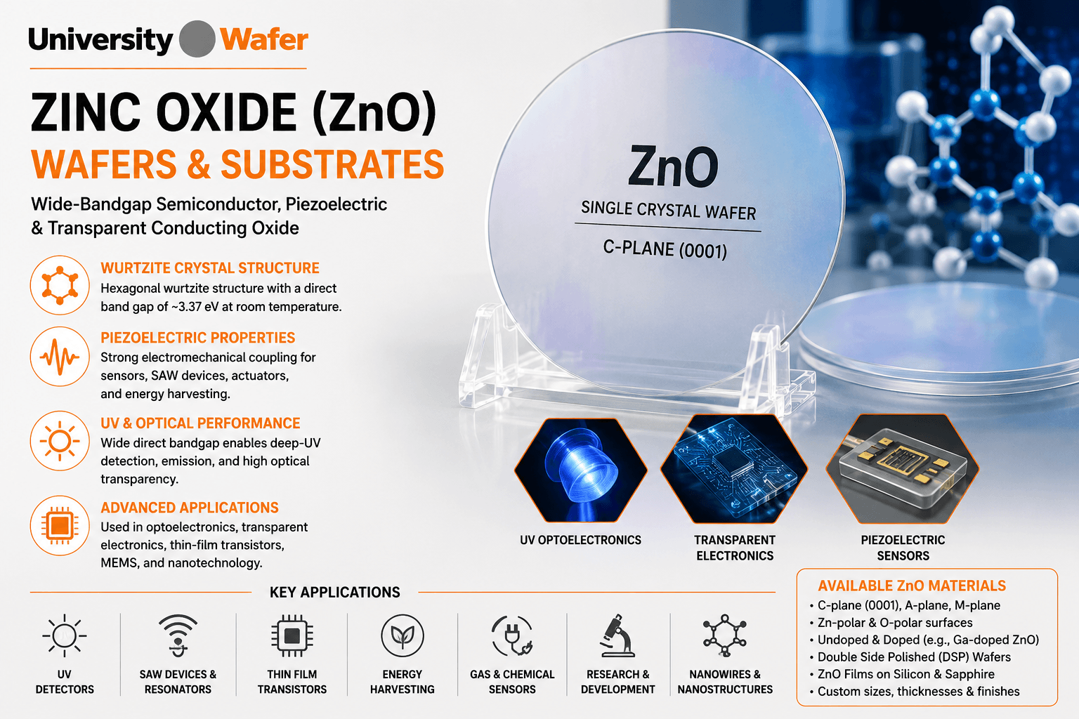
Zinc oxide (ZnO) wafers are crystalline substrates used in semiconductor, optoelectronic, piezoelectric, photonic, and sensor research. ZnO is a II-VI compound semiconductor that normally crystallizes in the hexagonal wurtzite structure. At room temperature, it has a direct band gap of approximately 3.37 eV, making it an important material for ultraviolet and wide-bandgap semiconductor research.
Unlike silicon, ZnO is both a semiconductor and a piezoelectric material. Its combination of optical transparency, wide direct band gap, and electromechanical response makes ZnO substrates useful for research involving UV photodetectors, acoustic-wave devices, sensors, transparent electronics, thin-film structures, and nanoscale devices.
Single-Crystal ZnO Substrates
Single-crystal zinc oxide substrates are available in different crystallographic orientations and surface configurations. Common orientations include c-plane (0001), A-plane (11-20), and M-plane (1-100). The appropriate orientation depends on the epitaxial relationship, polarization behavior, surface chemistry, and device structure required by the experiment.
Polar c-plane ZnO can also be prepared with either Zn-terminated or O-terminated surfaces. Surface termination is particularly important in epitaxy and surface-science experiments because it can influence surface reconstruction, adsorption, interface formation, and thin-film nucleation. UniversityWafer supplies ZnO configurations for researchers who require specific orientations, surface finishes, or doped material.
ZnO as a Wide-Bandgap Semiconductor
The direct band gap of ZnO makes the material especially interesting for short-wavelength optoelectronics. Researchers study ZnO semiconductors for ultraviolet emitters and detectors, photonic structures, heterostructures, and other devices where direct electronic transitions are advantageous.
ZnO also has a relatively large exciton binding energy of approximately 60 meV, which has contributed to substantial research into excitonic and light-emitting phenomena at and above room temperature. Researchers studying semiconductor band structures can learn more about semiconductor band gaps and their role in electronic and optoelectronic devices.
Piezoelectric ZnO for Sensors and Acoustic Devices
Wurtzite ZnO lacks inversion symmetry and therefore exhibits piezoelectric behavior. Mechanical deformation can produce electrical polarization, while an applied electric field can produce mechanical deformation. This electromechanical coupling makes ZnO useful for surface acoustic wave (SAW) devices, resonators, pressure and vibration sensors, MEMS structures, and energy-harvesting research.
ZnO thin films and nanostructures are also extensively investigated for nanoscale piezoelectric generators and multifunctional sensors. Researchers developing these structures can explore substrates for ZnO nanowire growth and related nanoscale device research.
ZnO for Transparent Electronics
Zinc oxide is transparent across much of the visible spectrum when prepared with appropriate composition and thickness. Its electrical conductivity can also be modified through doping and defect control. For example, Ga-doped ZnO can provide substantially greater conductivity than nominally undoped ZnO while retaining useful optical transparency.
These properties make ZnO and doped ZnO films relevant to transparent electrodes, thin-film transistors, displays, photovoltaic structures, and other transparent electronic devices. The electrical and optical properties depend strongly on carrier concentration, defects, dopants, film thickness, crystal quality, and deposition conditions.
ZnO Thin Films on Silicon and Sapphire
Researchers do not always require a bulk ZnO crystal. Zinc oxide can also be deposited as a thin film on other substrate materials. UniversityWafer supplies and supports ZnO on silicon wafers for MEMS, sensors, photodetectors, thin-film transistors, and other semiconductor experiments.
Another option is ZnO epitaxial films on sapphire . Sapphire provides an electrically insulating and thermally stable platform for ZnO thin-film and heteroepitaxial research. The resulting film quality depends on factors including substrate orientation, surface preparation, deposition technique, temperature, and growth conditions.
Zinc Oxide Wafer Applications
Depending on crystal orientation, doping, surface finish, and device structure, ZnO wafers and zinc oxide substrates are studied for applications including:
- Ultraviolet photodetectors and optoelectronics
- Surface acoustic wave (SAW) devices
- Piezoelectric sensors and actuators
- Thin-film transistors (TFTs)
- Transparent electronic structures
- Gas and chemical sensors
- MEMS and microsensor research
- Photovoltaic and photoelectrochemical research
- ZnO nanowires and nanostructures
- Thin-film and heteroepitaxial growth studies
UniversityWafer supplies zinc oxide wafers, ZnO crystals, doped ZnO substrates, and ZnO thin-film structures for university, government, and industrial research. Specify the required orientation, dimensions, surface termination, polish, doping, and quantity when requesting material for a particular experiment.
Get Your Zinc Oxide (ZnO) Quote FAST!
Or, Buy Wafers Online
and Start Researching Today!
Choosing the Right Zinc Oxide (ZnO) Substrate
Selecting a zinc oxide (ZnO) wafer requires careful consideration of crystal orientation, polarity, doping, surface finish, thickness, dimensions, and the intended fabrication process. These parameters can affect epitaxial growth, electrical behavior, optical response, piezoelectric performance, and interface quality.
For thin-film and epitaxial research, surface quality is especially important. A polished single-crystal ZnO substrate provides a well-defined crystalline surface for studying interfaces, heterostructures, semiconductor films, and nanoscale materials. Researchers should select substrate specifications according to the requirements of the deposition method and final device architecture.
ZnO Crystal Orientation and Polarity
ZnO normally crystallizes in the hexagonal wurtzite structure. Because this structure lacks inversion symmetry, crystallographic orientation and polarity can strongly influence surface and electromechanical behavior. Common ZnO substrate orientations include c-plane (0001), A-plane (11-20), and M-plane (1-100).
The c-axis is polar, and c-plane ZnO crystals can present either a Zn-polar or O-polar surface depending on the crystal termination. These two surfaces can exhibit different chemical reactivity, growth kinetics, surface morphology, and interface behavior. For this reason, specifying the required polarity can be important for ZnO epitaxy, surface-science studies, and heterostructure development.
C-Plane ZnO for Epitaxial Research
C-plane ZnO substrates are widely studied for homoepitaxial ZnO growth and for heteroepitaxial structures involving other wurtzite materials. Their well-defined (0001) orientation makes them useful for investigating polarization effects, interfaces, quantum structures, and wide-bandgap semiconductor devices.
Researchers can also use other substrate materials for ZnO deposition. For example, ZnO epitaxial films on sapphire provide an alternative platform for optoelectronic, sensor, and thin-film research. Sapphire is electrically insulating and thermally stable, although lattice and thermal-expansion differences between ZnO and sapphire must be considered during heteroepitaxial growth.
Undoped and Doped ZnO Materials
Nominally undoped ZnO typically exhibits n-type conductivity, although its electrical behavior depends strongly on native defects, unintentional impurities, growth conditions, and processing history. Controlling carrier concentration is therefore an important part of ZnO semiconductor research.
ZnO can also be intentionally doped to modify its electrical properties. Group-III dopants such as gallium or aluminum are commonly investigated as donors for increasing n-type conductivity. Ga-doped ZnO and Al-doped ZnO (AZO) are particularly relevant to transparent conducting oxide research because suitable films can combine visible-light transparency with useful electrical conductivity.
Researchers studying how doping changes semiconductor behavior can learn more about doping and carrier mobility . Although the linked discussion focuses on silicon, the underlying concepts of dopant concentration, carrier scattering, and electrical transport are also important when evaluating other semiconductor systems.
ZnO Thin-Film Deposition
Zinc oxide thin films can be prepared using several deposition techniques, including sputtering, pulsed laser deposition (PLD), chemical vapor deposition (CVD), molecular beam epitaxy (MBE), and atomic layer deposition (ALD) . The appropriate technique depends on the required film thickness, crystallinity, conformality, composition, interface quality, and substrate compatibility.
Atomic layer deposition of ZnO is particularly useful when precise thickness control and conformal coverage are required. ALD uses sequential, self-limiting surface reactions to build films cycle by cycle, making it suitable for planar surfaces as well as certain high-aspect-ratio structures.
For experiments requiring ZnO deposited directly onto a conventional semiconductor platform, researchers can explore ZnO on silicon wafers for sensors, MEMS, optoelectronics, and thin-film device development.
ZnO Nanowires and Nanostructures
ZnO is extensively studied in nanostructured forms including nanowires, nanorods, nanoparticles, and nanosheets. ZnO nanowires are of particular interest because their high surface-to-volume ratio and semiconducting, optical, and piezoelectric properties can be useful in nanosensors, photodetectors, energy-harvesting structures, and nanoscale electronic devices.
Researchers developing one-dimensional ZnO structures can explore substrates for ZnO nanowire growth and related materials for nanoscale semiconductor experiments.
ZnO for UV Optoelectronics and Photodetectors
ZnO has a direct room-temperature band gap of approximately 3.3–3.4 eV, corresponding to the near-ultraviolet region. This makes ZnO attractive for research into UV photodetectors, short-wavelength optoelectronics, light-emitting structures, and photonic devices.
Device performance depends on much more than the bulk band gap. Crystal defects, surface states, interfaces, carrier concentration, contact design, film thickness, and processing conditions can all influence the electrical and optical response of a ZnO photodetector or optoelectronic structure.
ZnO for Piezoelectric and Acoustic-Wave Devices
The non-centrosymmetric wurtzite crystal structure gives ZnO useful piezoelectric properties. ZnO films and crystals can therefore convert mechanical deformation into electrical polarization and can also deform mechanically in response to an applied electric field.
This behavior supports research involving surface acoustic wave (SAW) devices, bulk acoustic wave resonators, MEMS sensors, actuators, ultrasonic transducers, and piezoelectric energy-harvesting structures. Orientation, film texture, electrode geometry, and crystalline quality are important parameters when optimizing electromechanical coupling.
ZnO Substrate Surface Preparation
Surface preparation can have a major influence on epitaxy and thin-film growth. Researchers may require polished ZnO wafers with controlled surface roughness, specified crystal orientation, and defined polarity. Double-side polished (DSP) material can be useful for optical transmission, backside processing, and experiments requiring access to both wafer surfaces.
Before ordering a ZnO wafer, researchers should consider specifications such as:
- Crystal orientation: c-plane, A-plane, M-plane, or custom
- Polarity: Zn-face or O-face when applicable
- Doping: nominally undoped or intentionally doped
- Electrical properties: resistivity or carrier concentration requirements
- Thickness and dimensions: matched to handling and processing needs
- Surface finish: single-side or double-side polished
- Surface roughness: selected for the intended deposition or epitaxial process
- Quantity: research quantities through larger production requirements when available
ZnO and Other Wide-Bandgap Semiconductor Materials
Zinc oxide belongs to a broader family of wide-bandgap materials investigated for high-performance electronics, optoelectronics, sensors, and photonics. Depending on the application, researchers may also compare ZnO with gallium nitride (GaN) wafers , silicon carbide (SiC) wafers , and other advanced semiconductor substrates.
Each material offers different band structures, thermal properties, electrical characteristics, crystal structures, and processing requirements. Selecting the appropriate substrate should therefore be based on the electrical, optical, mechanical, and epitaxial requirements of the specific experiment rather than band gap alone.
Get Your Zinc Oxide (ZnO) Quote FAST!
Or, Buy Wafers Online
and Start Researching Today!
Related Zinc Oxide & Semiconductor Materials
- Zinc Oxide (ZnO) on Silicon Wafers – Explore ZnO thin films on silicon for sensors, MEMS, optoelectronics, and semiconductor research.
- ZnO Epitaxial Films on Sapphire – ZnO-on-sapphire structures for epitaxy, optoelectronics, sensors, and thin-film materials research.
- ZnO Nanowires – Substrates and materials for zinc oxide nanowire growth, nanosensors, photodetectors, and nanotechnology research.
- Atomic Layer Deposition (ALD) – Learn about ALD for precisely controlled and conformal semiconductor and oxide thin-film deposition.
- Semiconductor Band Gap – Learn how semiconductor band gaps influence optical absorption, carrier excitation, and device applications.
- Gallium Nitride (GaN) Wafers – Explore another direct wide-bandgap semiconductor used for optoelectronics, RF devices, and power electronics.
- Silicon Carbide (SiC) Wafers – Wide-bandgap SiC substrates for power electronics, high-temperature devices, and advanced semiconductor research.
- Semiconductor Wafers & Substrates – Browse semiconductor substrate materials for electronic, photonic, sensor, and materials-science applications.