
What Is a Semiconductor Wafer?
A semiconductor wafer is a thin, typically single-crystal substrate used as the starting material or supporting platform for electronic, photonic, sensing, and microfabricated devices. Semiconductor materials have electrical conductivity between that of good conductors and good insulators, and their electrical properties can be engineered through doping, temperature, electric fields, optical excitation, material composition, and device structure.
Semiconductor wafers provide the crystalline foundation on which processes such as epitaxy, oxidation, thin-film deposition, photolithography, etching, ion implantation, diffusion, metallization, and wafer bonding can be performed.
Different semiconductor substrate materials provide different band structures, carrier transport properties, breakdown fields, thermal characteristics, optical responses, and lattice parameters. Selecting the correct material is therefore an important first step in semiconductor device design.
Why Silicon Is the Most Widely Used Semiconductor
Silicon wafers are the dominant substrates for integrated circuits and many other semiconductor technologies. Silicon combines a mature manufacturing infrastructure with good mechanical properties, controllable doping, and the ability to form a high-quality native oxide, silicon dioxide (SiO2).
The Si/SiO2 materials system has been especially important to metal-oxide-semiconductor (MOS) technology and the development of modern integrated circuits. Silicon is also widely used for MEMS, sensors, photovoltaics, detectors, microfluidics, thin-film research, and numerous laboratory applications.
Single-crystal silicon wafers are available with different crystal orientations, conductivity types, dopants, resistivities, diameters, thicknesses, and surface finishes. These specifications should be selected according to the intended fabrication process rather than treating all silicon substrates as interchangeable.
Single-Crystal Semiconductor Substrates
Many semiconductor devices are fabricated on single-crystal substrates. In a single crystal, the atomic lattice maintains a continuous crystallographic orientation through the crystalline region rather than being divided into many differently oriented grains.
Crystal orientation can affect etching behavior, epitaxial growth, surface structure, mechanical properties, and some electronic characteristics. Common silicon orientations include (100), (110), and (111), with (100) silicon being especially common in semiconductor processing.
P-Type and N-Type Semiconductor Wafers
The electrical properties of semiconductor materials can be intentionally modified through doping. In silicon, p-type silicon is commonly produced using boron as an acceptor dopant, making holes the majority carriers.
N-type silicon commonly uses donor dopants such as phosphorus, arsenic, or antimony, making electrons the majority carriers.
P-type and n-type do not mean that the bulk semiconductor carries a net positive or negative electrical charge. The terms identify the dominant mobile carrier type under equilibrium conditions in the doped material.
Silicon Wafer Resistivity
Wafer resistivity, typically expressed in ohm-centimeters (Ω·cm), is an important specification for semiconductor substrates. In doped silicon, resistivity depends on carrier concentration and carrier mobility.
Increasing the electrically active dopant concentration generally decreases resistivity, although the relationship is not perfectly linear because carrier mobility also varies with doping concentration and temperature.
Researchers can use silicon resistivity and dopant-density data when selecting substrates for electrical, device, MEMS, detector, and semiconductor-processing applications.
Silicon-on-Insulator (SOI) Wafers
Silicon-on-Insulator (SOI) wafers are engineered substrates consisting of a crystalline silicon device layer separated from a silicon handle wafer by an insulating layer, commonly a buried silicon dioxide layer known as the buried oxide (BOX).
SOI enables electrical isolation between the device layer and handle substrate and provides precise control over the thickness of the active silicon layer. These properties make SOI useful for CMOS research, MEMS, RF devices, photonics, sensors, and other applications.
What Are Compound Semiconductors?
Compound semiconductors are formed from two or more chemical elements rather than a single elemental semiconductor such as silicon or germanium. Important examples include III-V materials such as gallium arsenide (GaAs), indium phosphide (InP), and gallium nitride (GaN).
Compound semiconductors can provide electronic and optical properties that differ substantially from silicon. Depending on the material, these can include direct band gaps, high electron transport performance, wide band gaps, and wavelength ranges useful for light emission or detection.
This makes III-V semiconductor materials important for RF electronics, LEDs, laser diodes, photodetectors, high-speed electronics, photovoltaics, and integrated photonics.
Gallium Arsenide (GaAs) Wafers
Gallium arsenide (GaAs) is a III-V compound semiconductor with a direct band gap near room temperature. Its electronic and optical properties make GaAs useful for high-frequency electronics and optoelectronic devices.
GaAs is used in applications including RF and microwave devices, laser diodes, LEDs, photodetectors, high-efficiency multijunction solar cells, and specialized high-speed electronics.
GaAs substrates can be supplied as conductive or semi-insulating material depending on the application. Semi-insulating GaAs provides high substrate resistivity, which is valuable for reducing unwanted electrical coupling in many RF and microwave device architectures.
Indium Phosphide (InP) Wafers
Indium phosphide (InP) is another direct-band-gap III-V semiconductor. It is particularly important as a substrate and epitaxial platform for high-speed electronics and optoelectronics.
InP-based material systems are widely used for lasers, photodetectors, modulators, photonic integrated circuits, and high-frequency devices. InP is also an important substrate for lattice-matched or near-lattice-matched epitaxial materials such as certain compositions of InGaAs and InGaAsP.
Wide-Bandgap Semiconductor Materials
Wide-bandgap semiconductors have larger band gaps than conventional silicon and are important for applications requiring high electric fields, elevated temperatures, high-frequency operation, or short-wavelength optoelectronics.
Two of the most important wide-bandgap semiconductor material systems are silicon carbide (SiC) and gallium nitride (GaN).
Their larger critical electric fields compared with silicon enable device architectures designed for high-voltage and high-power operation, although actual device performance also depends on material quality, thermal design, contacts, epitaxial structure, processing, and device geometry.
Silicon Carbide (SiC) Wafers
Silicon carbide is a wide-bandgap semiconductor available in multiple crystal polytypes. 4H-SiC is particularly important for modern power-electronic devices.
SiC combines a wide band gap, high critical electric field, and relatively high thermal conductivity. These characteristics make SiC attractive for power MOSFETs, Schottky diodes, high-temperature electronics, sensors, and other devices designed for demanding electrical or thermal environments.
SiC is also used as a substrate for some GaN epitaxial structures because its thermal properties can be advantageous for high-power RF applications.
Gallium Nitride (GaN) Semiconductor Wafers
Gallium nitride (GaN) is a direct, wide-bandgap III-V semiconductor used in power electronics, RF and microwave devices, LEDs, laser diodes, and optoelectronics.
GaN device layers can be grown on substrates including sapphire, silicon, and silicon carbide. The substrate influences factors such as thermal management, lattice mismatch, wafer cost, achievable diameter, stress, and integration strategy.
AlGaN/GaN heterostructures are particularly important for high-electron-mobility transistors (HEMTs) used in RF and power-electronic research.
Germanium Semiconductor Wafers
Germanium (Ge) is an elemental semiconductor with a smaller band gap than silicon and high carrier mobilities. Germanium played an important role in early transistor technology and remains useful in modern semiconductor and optical research.
Applications include infrared optics and detectors, specialized semiconductor devices, multijunction photovoltaics, and germanium-on-silicon structures for photonic and electronic research.
Silicon Germanium (SiGe)
Silicon germanium (SiGe) is a semiconductor alloy system whose properties can be engineered by changing the silicon-to-germanium composition.
SiGe is particularly important for heterojunction bipolar transistors, BiCMOS technologies, strained-layer structures, infrared photonics, and research involving band-structure and strain engineering.
Semiconductor Substrates vs. Insulating Substrates
Not every wafer used in semiconductor fabrication is itself a semiconductor. Materials such as sapphire, fused silica, quartz, and many glasses are electrically insulating substrates but can still play important roles in semiconductor and photonic device fabrication.
For example, sapphire wafers can serve as substrates for GaN epitaxy and other optical or electronic structures. Sapphire should therefore be described as an important semiconductor-industry substrate, not as a semiconductor material itself.
How to Choose a Semiconductor Wafer
Choosing the right semiconductor substrate requires matching material properties and wafer specifications to the intended device and fabrication process. Important parameters can include:
- Material – Si, Ge, GaAs, InP, SiC, GaN, SiGe, or another semiconductor
- Wafer diameter – based on equipment and process compatibility
- Thickness and thickness tolerance
- Crystal orientation
- Conductivity type – p-type, n-type, semi-insulating, or undoped where applicable
- Dopant species and concentration
- Electrical resistivity
- Surface finish – SSP or DSP
- Surface roughness
- Total Thickness Variation (TTV)
- Bow and warp
- Epitaxial layer structure when required
- Optical and electrical properties required by the application
The correct specification depends on the intended process. A wafer optimized for CMOS research may require very different electrical and geometric properties from a substrate intended for RF electronics, photonics, MEMS, power devices, or epitaxial growth.
Semiconductor Wafers for Research and Device Development
UniversityWafer supplies semiconductor wafers and specialty substrates for university, government, and industrial research, including silicon, SOI, GaAs, InP, SiC, GaN, germanium, SiGe, sapphire, glass, quartz, and engineered wafer structures.
Researchers can select substrates according to material, diameter, thickness, crystal orientation, conductivity type, resistivity, polishing, epitaxial structure, and other specifications required for semiconductor fabrication, microelectronics, photonics, MEMS, sensors, RF devices, and power electronics.
Get Your Semiconductor Wafer Quote FAST!
Or, Buy Wafers Online
and Start Researching Today!
How Semiconductor Material Properties Affect Device Performance
Selecting a semiconductor material requires more than comparing wafer diameter or price. Fundamental properties such as band gap, carrier mobility, critical electric field, thermal conductivity, dielectric properties, lattice constant, and optical absorption influence which materials are suitable for a particular device.
Semiconductor band gap is especially important because it influences intrinsic carrier concentration, optical absorption and emission, leakage behavior, and the temperature range over which a material can be useful. Silicon has an indirect band gap of approximately 1.12 eV near room temperature, while materials such as GaAs and GaN have direct band gaps.
Direct-band-gap semiconductors are particularly useful for efficient light emission because electron-hole recombination can occur without requiring the same phonon-assisted momentum change needed for indirect-gap silicon. This is one reason III-V materials are widely used for LEDs and semiconductor lasers.
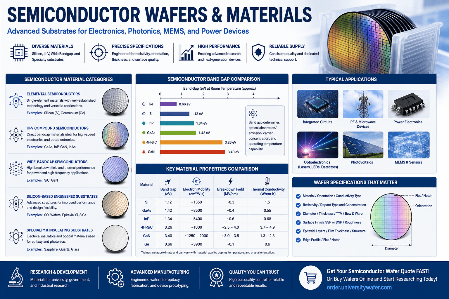
Semiconductor Band Gap Comparison
Different semiconductor materials cover substantially different band-gap ranges. Approximate room-temperature values for several important materials include:
- Germanium (Ge): ~0.66 eV, indirect
- Silicon (Si): ~1.12 eV, indirect
- Indium Phosphide (InP): ~1.34 eV, direct
- Gallium Arsenide (GaAs): ~1.42 eV, direct
- 4H-Silicon Carbide (4H-SiC): ~3.26 eV, indirect
- Gallium Nitride (GaN): ~3.4 eV, direct
These values are approximate and vary with temperature, composition, strain, crystal polytype, and other material conditions. Band gap alone does not determine device performance, but it is a useful starting point when comparing semiconductor materials and their band gaps.
Elemental vs. Compound Semiconductors
Elemental semiconductors are composed primarily of one semiconductor element. Silicon and germanium are the most important examples used as crystalline wafer materials.
Compound semiconductors contain multiple elements. III-V semiconductors combine elements primarily from groups 13 and 15 of the periodic table and include GaAs, InP, GaN, GaSb, and InAs. Other technologically important compound semiconductors include SiC and II-VI materials.
Compound semiconductors expand the range of available band gaps, lattice constants, carrier-transport properties, and optical characteristics, enabling devices that would be difficult to optimize using silicon alone.
III-V Semiconductor Wafers
III-V semiconductor wafers are particularly important for optoelectronics and high-frequency electronics. Many III-V materials have direct band gaps and favorable electron-transport properties.
Gallium arsenide (GaAs) is widely used for RF electronics, microwave devices, LEDs, laser diodes, photodetectors, and high-efficiency multijunction photovoltaic cells.
Indium phosphide (InP) provides a platform for high-speed electronic and photonic devices, including lasers and photodetectors used at important fiber-optic telecommunications wavelengths when combined with suitable epitaxial materials such as InGaAs and InGaAsP.
Wide-Bandgap Semiconductors for Power Electronics
Wide-bandgap semiconductor materials such as SiC and GaN have become important for power electronics because their high critical electric fields can enable devices that withstand high voltages with thinner or more heavily doped drift regions than comparable silicon designs.
4H-SiC wafers are particularly important for high-voltage power MOSFETs and Schottky barrier diodes. SiC also has relatively high thermal conductivity, which is beneficial for thermal management in high-power devices.
Gallium nitride (GaN) is used for high-frequency and power-electronic devices as well as LEDs and laser diodes. GaN-based heterostructures can support high-density two-dimensional electron gases used in high-electron-mobility transistors (HEMTs).
GaN-on-Silicon, GaN-on-Sapphire, and GaN-on-SiC
GaN is frequently grown heteroepitaxially on substrates other than bulk GaN. The substrate influences wafer size, thermal behavior, stress, defect formation, processing compatibility, and cost.
GaN-on-sapphire is widely associated with LED and optoelectronic technologies. Sapphire is electrically insulating and optically transparent over a broad wavelength range, although its lattice and thermal properties differ substantially from GaN.
GaN-on-silicon can leverage larger-diameter silicon substrates and established silicon manufacturing infrastructure, but differences in lattice parameters and thermal expansion coefficients require carefully engineered buffer layers and stress management.
GaN-on-SiC is particularly attractive for high-power-density RF devices because SiC provides high thermal conductivity. Each platform therefore addresses a different combination of performance, processing, and economic requirements.
Semiconductor Materials for RF and Microwave Devices
High-frequency devices require careful consideration of carrier transport, parasitic capacitance, substrate resistivity, thermal management, breakdown behavior, and device architecture.
GaAs has long been important for RF and microwave electronics, while InP-based technologies are used for very-high-frequency and high-speed devices. GaN-based HEMTs are particularly important when high RF output power and high electric-field capability are required.
Silicon technologies, including high-resistivity silicon and SOI, are also important RF platforms because they can provide high levels of integration with mature CMOS processing.
Semiconductor Materials for Photonics
Semiconductor materials interact with light in ways determined by their electronic band structures and optical constants. Direct-band-gap III-V semiconductors are especially important for efficient light emission, while silicon has become a major platform for passive and active silicon photonics.
Silicon-on-insulator is widely used for photonic waveguides because the refractive-index contrast between silicon and silicon dioxide enables strong optical confinement. Germanium and III-V materials can be integrated with silicon platforms to provide additional photodetection, modulation, or light-generation functionality.
Semiconductor Materials for Photodetectors
The spectral response of a semiconductor photodetector is strongly influenced by its band gap. Photons generally must have sufficient energy to generate electron-hole pairs through the relevant absorption process.
Silicon is widely used for visible and near-infrared photodetection within its useful spectral response range. Germanium and narrow-band-gap semiconductors such as InAs extend detection capabilities toward longer infrared wavelengths.
Detector material selection should consider not only band gap but also dark current, absorption coefficient, operating temperature, noise, device architecture, and the target wavelength range.
Semiconductor Materials for Solar Cells
Photovoltaic devices convert absorbed photon energy into electrical power through semiconductor junctions and selective contacts.
Crystalline silicon dominates terrestrial photovoltaic manufacturing because of its material availability, established manufacturing infrastructure, long-term stability, and mature device technology.
III-V materials such as GaAs and related alloys can achieve very high conversion efficiencies and are especially important in multijunction and space photovoltaic applications, although their substrate and fabrication costs are generally higher than those of conventional silicon photovoltaics.
Semiconductor Wafers for MEMS and Sensors
Silicon MEMS wafers are used to fabricate accelerometers, pressure sensors, gyroscopes, microphones, resonators, actuators, and other microelectromechanical devices.
Single-crystal silicon is particularly useful as a mechanical material because of its predictable elastic behavior and compatibility with precision micromachining. SOI wafers can provide a controlled silicon device-layer thickness and buried oxide useful for many MEMS structures.
Other semiconductor materials can be selected when MEMS devices require piezoresistive, optical, high-temperature, RF, or harsh-environment characteristics beyond those provided by conventional silicon.
High-Resistivity Semiconductor Wafers
High-resistivity silicon wafers contain relatively low concentrations of electrically active dopants and are used when low substrate conductivity is desirable.
Applications can include RF research, detectors, high-voltage structures, photonics, and certain sensor technologies. High-resistivity Float-Zone silicon is particularly important because the FZ process can produce silicon with very low concentrations of oxygen and other impurities compared with typical Czochralski-grown material.
Semiconductor Wafer Crystal Growth
Semiconductor wafer quality begins with crystal growth. Silicon is commonly manufactured using the Czochralski (CZ) process or the Float-Zone (FZ) method.
Compound semiconductor crystals require growth methods suited to their chemistry, vapor pressure, phase behavior, and desired crystal quality. Substrate manufacturing can include crystal growth, orientation, slicing, edge shaping, lapping, etching, polishing, cleaning, and inspection before the wafer is ready for device processing or epitaxy.
Epitaxial Semiconductor Wafers
Epitaxy is the growth of a crystalline layer whose crystallographic relationship is influenced by the underlying crystalline substrate. Epitaxial layers allow device engineers to control material composition, thickness, doping, strain, and heterostructure design.
Epitaxial silicon wafers can contain device layers with different doping levels from the underlying silicon substrate. Compound-semiconductor epitaxy can create multilayer heterostructures such as AlGaAs/GaAs, InGaAs/InP, and AlGaN/GaN.
Techniques including chemical vapor deposition (CVD), metal-organic chemical vapor deposition (MOCVD), and molecular beam epitaxy (MBE) are used for different semiconductor material systems.
Semiconductor Wafer Surface Finish
Surface condition is critical because semiconductor processing often begins directly on the polished wafer surface. Single-side polished (SSP) wafers provide a high-quality polished surface on one side, while double-side polished (DSP) wafers provide polished surfaces on both sides.
DSP substrates are useful for applications involving backside lithography, transmission optics, wafer bonding, MEMS, double-sided processing, and other processes where both surfaces are functionally important.
Wafer Geometry and Total Thickness Variation
Semiconductor substrate quality also depends on geometric specifications. Total Thickness Variation (TTV) describes the difference between the maximum and minimum local thickness values across a wafer under the applicable measurement conditions.
TTV is distinct from bow and warp, which describe aspects of wafer shape rather than local thickness variation. These parameters can influence lithography, bonding, grinding, polishing, epitaxy, handling, and other precision semiconductor processes.
Semiconductor Wafer Orientation
Crystal orientation describes the crystallographic plane associated with the wafer surface. Silicon substrates commonly use (100), (110), or (111) orientations.
Orientation can influence anisotropic etching, surface atomic structure, epitaxial relationships, mechanical properties, ion implantation channeling, and device processing. The correct orientation should therefore be chosen according to the fabrication process and device architecture.
Choosing Between Silicon, GaAs, InP, SiC, and GaN
There is no universally superior semiconductor wafer material. Each substrate provides a different combination of electronic, optical, thermal, mechanical, and manufacturing characteristics.
- Silicon (Si) – mature processing, excellent SiO2 interface technology, CMOS, MEMS, sensors, photovoltaics, and photonics.
- Gallium Arsenide (GaAs) – direct band gap, RF and microwave electronics, optoelectronics, lasers, LEDs, and high-efficiency solar cells.
- Indium Phosphide (InP) – photonic integrated circuits, telecom lasers and detectors, and high-speed electronics.
- Silicon Carbide (SiC) – high-voltage power electronics, high-temperature devices, and harsh-environment applications.
- Gallium Nitride (GaN) – RF electronics, power devices, LEDs, lasers, and wide-bandgap semiconductor research.
- Germanium (Ge) – infrared detectors and optics, silicon photonics integration, specialized electronics, and multijunction photovoltaic structures.
The final choice should be based on measurable device requirements rather than selecting a material solely because it has a larger band gap or higher carrier mobility.
How to Specify Semiconductor Wafers
When ordering semiconductor substrates, researchers should provide specifications that reflect both the device requirements and the fabrication equipment being used.
Important parameters can include:
- Semiconductor material or substrate stack
- Wafer diameter
- Wafer thickness and tolerance
- Crystal orientation
- Conductivity type
- Dopant species
- Resistivity or carrier concentration
- SSP or DSP surface finish
- Surface roughness
- TTV, bow, and warp requirements
- Epitaxial material and layer thickness
- Film or dielectric requirements
- Edge profile, flats, or notch requirements
Specifying only the semiconductor material is often insufficient. Electrical, crystallographic, surface, and geometric requirements can be equally important to whether a wafer is compatible with a particular experiment or fabrication process.
Semiconductor Substrates for Research and Development
UniversityWafer supplies semiconductor wafers and research substrates for electronics, photonics, MEMS, sensors, RF devices, power electronics, photovoltaics, epitaxial growth, thin-film deposition, and materials research.
Available substrate families include silicon, SOI, GaAs, InP, SiC, GaN, germanium, SiGe, and other semiconductor materials, as well as insulating substrates such as sapphire, quartz, fused silica, and glass for applications where those materials provide the required optical, thermal, electrical, or epitaxial properties.
Related Semiconductor Wafer Resources
- Semiconductor Wafers – Learn about semiconductor substrates used for electronics, photonics, MEMS, sensors, and advanced device fabrication.
- Silicon Wafers – Explore silicon substrates by diameter, orientation, resistivity, dopant, thickness, and surface finish.
- Silicon-on-Insulator (SOI) Wafers – Learn about SOI substrates with a crystalline silicon device layer, buried oxide (BOX), and silicon handle wafer.
- III-V Semiconductor Materials – Explore compound semiconductor substrates for RF electronics, photonics, optoelectronics, and high-speed devices.
- Gallium Arsenide (GaAs) Wafers – Explore GaAs substrates for RF and microwave electronics, lasers, LEDs, photodetectors, and photovoltaic research.
- Indium Phosphide (InP) Wafers – Learn about InP substrates for high-speed electronics, lasers, photodetectors, and photonic integrated circuits.
- Gallium Nitride (GaN) Wafers – Learn about wide-bandgap GaN semiconductor materials for power electronics, RF devices, LEDs, and optoelectronics.
- Germanium (Ge) Wafers – Explore germanium substrates for infrared detectors and optics, photovoltaics, photonics, and semiconductor research.
- Silicon Germanium (SiGe) – Learn about SiGe semiconductor structures for high-speed electronics, heterojunction devices, photonics, and strain engineering.
- Semiconductor Band Gap – Understand semiconductor band gaps and how they influence electrical and optical material behavior.
- High-Resistivity Silicon Wafers – Explore low-doped silicon substrates for RF, detectors, photonics, high-voltage structures, and specialized research.
- Epitaxial Silicon Wafers – Learn how crystalline epitaxial silicon layers provide controlled thickness, doping, and electrical properties for device fabrication.
- Silicon Wafer Crystal Orientation – Compare (100), (110), and (111) orientations and their importance in etching, epitaxy, implantation, MEMS, and semiconductor processing.
- Semiconductor Wafer Products – Browse semiconductor, compound semiconductor, insulating, optical, and specialty wafer materials for research and fabrication.