
LPCVD and PECVD Silicon Nitride Wafers for MEMS and Semiconductor Research
UniversityWafer, Inc. supplies silicon nitride wafers with LPCVD and PECVD films for MEMS fabrication, dielectric isolation, KOH etching, and semiconductor device manufacturing. We stock a wide range of nitride-coated silicon wafers in small and large quantities, allowing researchers to purchase as few as one wafer.
Our most popular nitride coatings include:
Stoichiometric LPCVD silicon nitride films are widely used as hard masks for KOH etching, oxidation barriers, and dielectric layers. These coatings are frequently used to define active regions during field oxidation and are compatible with a variety of MEMS and semiconductor processes.
Get Your Quote FAST! Or, Buy Online and Start Researching Today!
Advantages of Silicon Nitride
Silicon nitride exhibits excellent high-temperature strength, oxidation resistance, wear resistance, and low thermal expansion. These characteristics provide outstanding thermal shock resistance and make silicon nitride an important material for microelectronics, MEMS, sensors, and harsh-environment applications.
Bulk silicon nitride materials are commonly manufactured as:
- Reaction Bonded Silicon Nitride (RBSN)
- Hot Pressed Silicon Nitride (HPSN)
- Sintered Silicon Nitride (SSN)
UniversityWafer, Inc. can supply silicon nitride coatings with custom specifications including film thickness, stress level, substrate orientation, and wafer diameter.
Available Wafer Diameters
We can deposit LPCVD and PECVD silicon nitride films on silicon wafers with the following diameters:
- 25.4 mm (1 inch)
- 50.8 mm (2 inch)
- 76.2 mm (3 inch)
- 100 mm (4 inch)
- 150 mm (6 inch)
- 200 mm (8 inch)
- 300 mm (12 inch)
Custom diameters, film thicknesses, and stress levels are available upon request for research and development applications.
LPCVD and PECVD Silicon Nitride Wafers in Stock
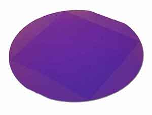 UniversityWafer, Inc. supplies silicon nitride wafers with LPCVD and PECVD films for MEMS fabrication, KOH etching, dielectric isolation, passivation layers, and semiconductor device manufacturing. We offer small and large quantities and can supply as few as one nitride-coated wafer.
Available silicon nitride coatings include:
- Stoichiometric LPCVD Silicon Nitride
- Low Stress Silicon Nitride
- Super Low Stress Silicon Nitride
- PECVD Silicon Nitride
- PECVD OxyNitride
- Low Stress PECVD Nitride
- PECVD Oxide
- PECVD Silicon Carbide
Stoichiometric LPCVD Silicon Nitride
Stoichiometric LPCVD silicon nitride provides excellent chemical resistance and dielectric properties. It is commonly used as a hard mask for KOH etching, an oxidation barrier, and a passivation layer in semiconductor devices. LPCVD nitride is also used to define active regions during field oxidation and for MEMS fabrication.
Low Stress Silicon Nitride
Low stress silicon nitride retains the electrical and chemical properties of standard nitride films while minimizing film stress. These coatings are widely used for MEMS devices, membranes, cantilever beams, pressure sensors, microfluidic structures, and other mechanical components that require dimensional stability.
Super Low Stress Silicon Nitride
Super low stress silicon nitride has been engineered for applications that require extremely low intrinsic stress. Film stress can be customized to meet specific requirements, making these wafers ideal for photonics, MEMS, suspended structures, and advanced sensor applications.
PECVD Silicon Nitride
PECVD silicon nitride is deposited at relatively low temperatures, making it suitable for wafers that cannot tolerate high-temperature processing. These single-sided films provide excellent flexibility and can be deposited over thermal oxide, TEOS oxide, metals, and other thin films.
PECVD OxyNitride
PECVD oxynitride combines the properties of silicon dioxide and silicon nitride to provide excellent dielectric performance and optical characteristics. It is frequently used in optical coatings, passivation layers, and semiconductor processing applications requiring low thermal budgets.
Low Stress PECVD Nitride
Low stress PECVD nitride provides improved mechanical stability while maintaining the advantages of low-temperature deposition. These films are commonly used in MEMS, sensors, and microelectronic devices that require reduced wafer bow and low residual stress.
PECVD Oxide Films
PECVD oxide films offer greater process flexibility than thermal oxide because they can be deposited at lower temperatures. These films are used for insulation layers, passivation coatings, interlayer dielectrics, and semiconductor device fabrication.
PECVD Silicon Carbide Coatings
PECVD silicon carbide coatings provide excellent chemical resistance, hardness, and electrical insulation. Low-temperature deposition allows these films to be integrated with other thin-film structures while minimizing thermal stress and process complexity.
Applications for Silicon Nitride Wafers
- MEMS devices and microsensors
- KOH etching hard masks
- Cantilever beams and membranes
- Passivation layers
- Dielectric isolation layers
- Photonic devices
- Microfluidic structures
- Pressure sensors
- Semiconductor fabrication
- Wafer-level packaging