What Are Acoustic Wave (SAW) Applications?
Acoustic wave devices, particularly Surface Acoustic Wave (SAW) devices, convert electrical signals into mechanical waves that travel across the surface of a piezoelectric substrate. Because these waves are highly sensitive to changes in mass, temperature, pressure, strain, and chemical interactions, SAW technology has become an essential platform for wireless sensors, RF filters, telecommunications, biosensors, microfluidics, automotive electronics, and semiconductor research.
UniversityWafer supplies high-quality wafer substrates for fabricating acoustic wave devices, including lithium niobate (LiNbO3), single crystal quartz, aluminum nitride (AlN), GaN on sapphire, silicon carbide (SiC), and sapphire wafers for research, prototyping, and production.
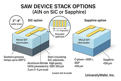
How Surface Acoustic Wave (SAW) Devices Work
A typical surface acoustic wave device consists of two interdigital transducers (IDTs) patterned onto a piezoelectric crystal. When an alternating electrical signal is applied to the transmitting IDT, the piezoelectric substrate converts the electrical energy into a mechanical surface wave. The receiving IDT converts the wave back into an electrical signal after it has propagated across the wafer surface.
Any change in the propagation path—including added mass, temperature variation, pressure, humidity, or chemical adsorption—alters the wave velocity, amplitude, or phase. Measuring these changes allows SAW devices to function as extremely sensitive sensors capable of detecting very small physical or chemical changes.
Why Piezoelectric Materials Are Used for SAW Devices
SAW devices require materials that exhibit strong piezoelectric properties. These materials generate an electric charge when mechanically stressed and deform when exposed to an electric field, allowing efficient conversion between electrical and acoustic energy.
Common substrates used for SAW fabrication include:
- Quartz — exceptional temperature stability and low signal loss.
- Lithium Niobate (LiNbO3) — high electromechanical coupling for filters, resonators, and wireless communication devices.
- Lithium Tantalate (LiTaO3) — excellent frequency stability and RF performance.
- Aluminum Nitride (AlN) — compatible with MEMS fabrication, high acoustic velocity, and excellent thermal stability.
- AlN on Silicon Carbide (SiC) — combines excellent heat dissipation with high-frequency operation for demanding RF applications.
- GaN on Sapphire — attractive for integrating acoustic devices with RF electronics and high-power semiconductor technologies.
Major Applications of Surface Acoustic Wave Technology
| Application |
Typical SAW Function |
| Wireless Communications |
RF filters, duplexers, resonators, and signal processing for smartphones, Wi-Fi, GPS, and 5G systems. |
| Automotive Electronics |
Pressure, torque, tire pressure, and wireless sensing in harsh environments. |
| Biosensors |
Detection of proteins, DNA, viruses, bacteria, and biomarkers through surface mass changes. |
| Chemical Sensors |
Detection of gases, volatile organic compounds (VOCs), humidity, and environmental contaminants. |
| Microfluidics |
Manipulation of droplets, cells, nanoparticles, and biological samples within lab-on-a-chip devices. |
| Industrial Monitoring |
Wireless monitoring of strain, temperature, vibration, and structural health. |
Advantages of Surface Acoustic Wave (SAW) Technology
Surface Acoustic Wave (SAW) devices have become a preferred technology for sensing and radio-frequency (RF) signal processing because they offer high sensitivity, compact size, excellent reliability, and low manufacturing cost. Since acoustic waves are confined to the surface of the substrate, even microscopic changes caused by added mass, mechanical strain, or chemical adsorption can produce measurable shifts in wave velocity, phase, or frequency.
Unlike many conventional sensors, SAW devices can operate passively without an onboard power source, making them attractive for wireless monitoring in environments where batteries are impractical. They are commonly deployed in industrial equipment, aerospace systems, automotive electronics, infrastructure monitoring, and medical devices where long-term stability and reliability are essential.
| Advantage |
Benefit |
| High Sensitivity |
Detects extremely small changes in mass, pressure, temperature, humidity, and strain. |
| Passive Operation |
No battery is required for many wireless sensing applications. |
| Small Size |
Ideal for MEMS devices, wearable electronics, and compact RF components. |
| High Frequency |
Operates from tens of MHz into the GHz range for modern communication systems. |
| Excellent Reliability |
Solid-state construction provides long operating life with minimal maintenance. |
| Low Power Consumption |
Suitable for portable electronics and remote monitoring applications. |
Common Substrate Materials for SAW Devices
The performance of a surface acoustic wave device depends heavily on the substrate material. Important material properties include acoustic velocity, electromechanical coupling coefficient, temperature coefficient of frequency (TCF), dielectric constant, thermal conductivity, and crystal orientation. Selecting the proper substrate is critical for achieving the desired operating frequency, signal stability, and environmental performance.
| Material |
Typical Applications |
Key Advantages |
| Quartz |
Precision oscillators, sensors, frequency control |
Excellent temperature stability and very low acoustic loss |
| Lithium Niobate (LiNbO₃) |
RF filters, duplexers, resonators |
High electromechanical coupling and excellent RF performance |
| Lithium Tantalate (LiTaO₃) |
Mobile communication filters |
High power handling and good frequency stability |
| Aluminum Nitride (AlN) |
MEMS, RF resonators, sensors |
High acoustic velocity, CMOS compatibility, and thermal stability |
| AlN on Silicon Carbide |
High-power RF electronics |
Excellent thermal conductivity and high-frequency operation |
| GaN on Sapphire |
RF and optoelectronic integration |
Supports integration with high-electron-mobility devices |
Interdigital Transducers (IDTs)
The heart of every SAW device is the interdigital transducer (IDT), a pattern of interlocking metal electrodes fabricated using standard semiconductor photolithography techniques. The spacing, width, and number of electrode fingers determine the operating frequency, bandwidth, insertion loss, and overall performance of the device.
Modern SAW components often use aluminum or gold IDTs fabricated on highly polished piezoelectric wafers. As semiconductor fabrication techniques continue to improve, researchers are developing increasingly complex IDT geometries to achieve higher frequencies, lower insertion loss, wider bandwidths, and improved sensor sensitivity for next-generation wireless communication and sensing applications.
Surface Acoustic Wave (SAW) Sensors for Chemical and Biosensing
One of the fastest-growing applications of Surface Acoustic Wave (SAW) technology is chemical and biological sensing. Because acoustic waves travel along the substrate surface, any interaction with molecules, cells, proteins, or gases causes measurable changes in wave velocity, phase, attenuation, or resonant frequency. This makes SAW sensors among the most sensitive label-free sensing technologies available.
Researchers commonly functionalize the surface with polymers, antibodies, enzymes, graphene, metal oxides, or other nanomaterials to selectively detect specific analytes. As target molecules bind to the sensing layer, the resulting mass loading alters the acoustic wave propagation, producing an electrical signal proportional to the concentration of the analyte.
| Application |
What the SAW Sensor Detects |
| Gas Sensors |
Hydrogen, methane, ammonia, VOCs, and other industrial gases. |
| Biosensors |
DNA, RNA, proteins, antibodies, viruses, bacteria, and biomarkers. |
| Environmental Monitoring |
Humidity, airborne contaminants, pollutants, and toxic chemicals. |
| Medical Diagnostics |
Disease biomarkers and point-of-care diagnostic testing. |
| Food Safety |
Bacterial contamination and chemical residues. |
SAW Devices for Wireless Communications
Modern wireless communication systems depend heavily on surface acoustic wave filters and resonators. SAW components are widely used to filter unwanted frequencies while allowing desired signals to pass with minimal insertion loss. Their compact size and excellent frequency stability make them indispensable in today's RF front-end modules.
Surface acoustic wave filters are commonly integrated into smartphones, tablets, satellite communication equipment, GPS receivers, Wi-Fi routers, Bluetooth devices, automotive radar, and emerging 5G and IoT platforms. As operating frequencies continue to increase, improved piezoelectric materials and optimized interdigital transducer (IDT) designs enable higher-performance RF filters with greater bandwidth and lower power consumption.
Surface Acoustic Wave (SAW) vs. Bulk Acoustic Wave (BAW) Devices
Although both SAW and Bulk Acoustic Wave (BAW) devices convert electrical energy into acoustic waves using piezoelectric materials, they differ in how the acoustic energy propagates. SAW devices confine the acoustic wave to the surface of the substrate, while BAW devices allow the wave to travel throughout the thickness of the material.
| Feature |
SAW Devices |
BAW Devices |
| Wave Propagation |
Along the substrate surface |
Through the bulk material |
| Typical Frequency |
10 MHz to several GHz |
Hundreds of MHz to over 10 GHz |
| Typical Applications |
Sensors, RF filters, biosensors, microfluidics |
High-frequency RF filters and power amplifiers |
| Fabrication |
Interdigital transducers on piezoelectric wafers |
Thin-film acoustic resonator structures |
| Major Advantage |
High sensitivity and simple fabrication |
Excellent high-frequency performance |
Current Research in Acoustic Wave Technology
Current research focuses on combining surface acoustic wave devices with advanced semiconductor materials such as graphene, gallium nitride (GaN), silicon carbide (SiC), and MEMS-compatible aluminum nitride (AlN). These material platforms improve acoustic velocity, thermal stability, power handling, and sensor sensitivity while enabling integration with modern semiconductor manufacturing processes.
As wireless sensing, wearable electronics, biomedical diagnostics, and Internet of Things (IoT) technologies continue to expand, SAW devices remain one of the most versatile and rapidly evolving classes of piezoelectric sensors available for both academic research and commercial product development.
Choosing the Right Wafer for Surface Acoustic Wave (SAW) Research
Selecting the proper SAW wafer substrate is one of the most important design decisions when fabricating surface acoustic wave devices. The substrate determines the acoustic velocity, electromechanical coupling coefficient, temperature stability, insertion loss, and overall device performance. Researchers typically choose a material based on the intended operating frequency, sensing environment, fabrication process, and application requirements.
UniversityWafer supplies a wide variety of piezoelectric wafers for SAW fabrication, including single crystal quartz, lithium niobate (LiNbO3), lithium tantalate (LiTaO3), sapphire, aluminum nitride (AlN), and GaN on sapphire for both research and commercial applications.
| Substrate |
Best For |
Main Advantage |
| Quartz |
Frequency control and precision sensors |
Excellent temperature stability and low acoustic loss |
| Lithium Niobate |
RF filters and resonators |
High electromechanical coupling coefficient |
| Lithium Tantalate |
Wireless communication devices |
High power handling and frequency stability |
| AlN on Silicon |
MEMS and integrated sensors |
CMOS compatible with high acoustic velocity |
| AlN on SiC |
High-power RF applications |
Excellent thermal conductivity |
| GaN on Sapphire |
High-frequency electronics |
Integration with RF and optoelectronic devices |
What Does SAW Grade Mean?
SAW grade refers to a piezoelectric wafer manufactured specifically for Surface Acoustic Wave device fabrication. These wafers are produced with tight control over crystal orientation, thickness uniformity, surface roughness, total thickness variation (TTV), and polishing quality to ensure consistent acoustic wave propagation.
Unlike standard optical or semiconductor-grade substrates, SAW-grade wafers are optimized for low acoustic loss and precise wave propagation. The selected crystal cut—such as ST-cut, AT-cut, or 128° Y-cut—directly influences temperature stability, acoustic velocity, and electromechanical performance, making crystal orientation one of the most important specifications for SAW device fabrication.
Quartz Wafers for Surface Acoustic Wave Devices
Single crystal quartz remains one of the most widely used materials for surface acoustic wave sensors, oscillators, timing devices, and precision frequency-control components. Its exceptional thermal stability, low signal attenuation, and excellent long-term reliability make it ideal for laboratory research as well as commercial RF products.
The following customer inquiry demonstrates the specifications commonly requested for high-performance SAW-grade quartz wafers.
Single Crystal Quartz Wafers for Surface Acoustic Wave (SAW) Devices
A researcher from a large U.S. university requested a quotation for SAW-grade single crystal quartz wafers to fabricate interdigital transducer (IDT) structures for surface acoustic wave devices. Their primary requirements included excellent crystal quality, reproducible thickness, low acoustic loss, and precise crystal orientation.
Researcher's Request:
We are interested in thin single crystal quartz wafers for fabricating surface acoustic wave devices.
- Material: Quartz (SAW Grade)
- Diameter: 4 inches
- Thickness: 100–150 μm (127 μm preferred)
- Lowest possible dielectric loss
- Excellent thickness uniformity
- Pricing and lead time requested
UniversityWafer supplies high-quality SAW-grade quartz wafers manufactured specifically for frequency-control devices, acoustic resonators, RF filters, and precision sensing applications. Standard orientations, custom crystal cuts, and research quantities are available upon request.
Understanding ST-Cut Quartz for SAW Devices
The ST-cut quartz wafer is one of the most widely used crystal orientations for surface acoustic wave (SAW) devices because it provides outstanding temperature stability while maintaining excellent acoustic performance. The crystal orientation determines how acoustic waves propagate through the substrate and directly affects wave velocity, insertion loss, and frequency stability.
Researchers frequently specify orientations such as ST-cut, AT-cut, or Z-cut, depending on whether the device is intended for sensors, resonators, oscillators, or RF filtering applications.
| Quartz Cut |
Typical Application |
Key Benefit |
| ST-Cut |
Surface acoustic wave devices |
Excellent temperature stability and low acoustic loss |
| AT-Cut |
Crystal oscillators |
High frequency stability |
| Z-Cut |
Optical and piezoelectric research |
Uniform crystal orientation |
Seeded vs. Seedless Quartz Wafers
Researchers often ask about the difference between seeded and seedless quartz crystals. Both materials provide excellent piezoelectric properties for SAW fabrication. The distinction refers to the crystal growth process rather than the electrical or acoustic performance of the finished wafer.
A seeded crystal is grown from a carefully oriented quartz seed crystal to control crystallographic direction during growth. Seedless quartz is produced using an alternative growth process and is often selected for applications requiring exceptional crystal uniformity. Both options are available depending on the device design and fabrication requirements.
The following specifications represent a typical SAW-grade quartz wafer supplied for research applications.
Gallium Nitride (GaN) on Sapphire Wafers for Surface Acoustic Wave Devices
Gallium nitride (GaN) on sapphire wafers are increasingly used for advanced Surface Acoustic Wave (SAW) and Bulk Acoustic Wave (BAW) devices because they combine the excellent piezoelectric properties of III-nitride materials with the mechanical stability and availability of sapphire substrates. These wafers are widely investigated for RF filters, wireless communication systems, high-frequency resonators, and harsh-environment sensors.
GaN offers excellent thermal stability, high acoustic velocity, wide bandgap characteristics, and compatibility with high-electron-mobility transistor (HEMT) technology. These properties make GaN-on-sapphire an attractive platform for integrating acoustic wave devices with high-power RF electronics and next-generation communication systems.
Researcher's Request
I would like to know the difference in material quality between 2 µm and 4 µm GaN epitaxial layers. The wafers will be used to fabricate surface acoustic wave (SAW) devices, so crystal uniformity, defect density, and film quality are important considerations.
UniversityWafer, Inc. replied:
Both 2 µm and 4 µm GaN epitaxial layers can provide excellent crystal quality for SAW device fabrication. The primary difference is the epitaxial layer thickness rather than the material quality. Depending on the device design, thicker GaN layers may offer additional flexibility for processing and acoustic wave engineering, while thinner layers are often selected for applications requiring tighter process control and reduced fabrication time.
UniversityWafer supplies custom GaN epitaxial wafers with various layer thicknesses, orientations, doping options, and substrate combinations for research and production applications.
| Feature |
Benefit for SAW Devices |
| Wide Bandgap |
Excellent performance at high temperature and high power. |
| High Acoustic Velocity |
Supports high-frequency resonators and RF filters. |
| Excellent Thermal Stability |
Suitable for harsh operating environments. |
| High Crystal Quality |
Improves acoustic wave propagation and device reliability. |
| HEMT Compatibility |
Allows integration with high-frequency RF electronics. |
Why Researchers Choose GaN for Acoustic Wave Research
Researchers developing next-generation 5G, 6G, radar, aerospace, defense, and wireless communication systems continue to investigate GaN-based acoustic devices because of their outstanding electrical and mechanical performance. When combined with optimized interdigital transducer (IDT) designs, GaN-on-sapphire structures enable compact, high-frequency SAW filters, resonators, and sensors capable of operating under demanding environmental conditions.
Typical research applications include RF front-end modules, wireless communication filters, biosensors, MEMS devices, pressure sensors, and integrated acoustic wave circuits where high power handling and thermal stability are required.
Reference #254146 for pricing.
Lithium Niobate (LiNbO3) Wafers for Surface Acoustic Wave (SAW) Devices
Lithium niobate (LiNbO3) is one of the most important piezoelectric materials used for Surface Acoustic Wave (SAW) devices. Its high electromechanical coupling coefficient, excellent acoustic properties, and ability to operate at microwave frequencies make it the preferred substrate for RF filters, resonators, delay lines, wireless communications, and precision sensing applications.
Compared with quartz, lithium niobate provides significantly stronger piezoelectric coupling, allowing designers to build smaller devices with wider bandwidth and higher operating frequencies. These characteristics have made LiNbO3 a standard material for smartphones, satellite communications, automotive radar, and emerging 5G and future 6G technologies.
Researcher's Request
We are interested in purchasing 128° Y-cut lithium niobate wafers for the fabrication of surface acoustic wave devices. Could you provide pricing, availability, and information regarding crystal quality, thickness tolerance, and lead time?
UniversityWafer supplies research-grade and production-grade lithium niobate wafers in multiple crystal orientations, diameters, thicknesses, and polishing options for SAW, optical, MEMS, and photonics research.
Why 128° Y-Cut Lithium Niobate Is Popular
Among the many available crystal orientations, 128° Y-cut LiNbO3 is one of the most commonly specified for SAW devices because it offers an excellent balance between acoustic velocity, electromechanical coupling, insertion loss, and frequency performance. It is widely used in RF filters, duplexers, oscillators, and high-performance resonators.
| Crystal Orientation |
Typical Application |
Main Advantage |
| 128° Y-Cut |
SAW filters and resonators |
High electromechanical coupling |
| Y-Cut |
General piezoelectric devices |
Balanced acoustic performance |
| X-Cut |
Optical and electro-optic devices |
Excellent optical properties |
| Z-Cut |
Nonlinear optics and photonics |
Strong electro-optic response |
Black vs. White Lithium Niobate Wafers
Researchers frequently ask about the difference between black and white lithium niobate. The distinction primarily relates to crystal appearance and manufacturing conditions rather than the fundamental piezoelectric behavior of the material. Both materials can be suitable for SAW fabrication depending on the device design and processing requirements.
When selecting a lithium niobate wafer, crystal orientation, surface finish, flatness, total thickness variation (TTV), and polishing quality are generally far more important than the wafer's appearance.
Typical Lithium Niobate Wafer Specifications
| Specification |
Typical Value |
| Diameter |
2", 3", 4", and custom sizes |
| Orientation |
128° Y-cut, X-cut, Y-cut, Z-cut |
| Surface Finish |
Single-side or double-side polished |
| Thickness |
Custom thicknesses available |
| TTV |
Available with tight research-grade tolerances |
| Edge Profile |
Standard or custom edge configurations |
Applications of Lithium Niobate SAW Devices
Lithium niobate substrates are widely used for manufacturing RF filters, duplexers, delay lines, resonators, biosensors, chemical sensors, microfluidic devices, MEMS sensors, oscillators, and precision timing components. Their combination of strong piezoelectric properties and excellent frequency response continues to make LiNbO3 one of the most versatile materials for acoustic wave technology.
Whether your research involves wireless communications, 5G infrastructure, IoT devices, biosensors, or high-frequency MEMS, UniversityWafer can supply high-quality lithium niobate, quartz, sapphire, GaN, aluminum nitride, and other piezoelectric wafer materials to support your project from prototype development through production.
Related Surface Acoustic Wave (SAW) Resources
