
Request SiC Wafers for Research and Device Fabrication
UniversityWafer supplies silicon carbide wafers for research, prototyping and semiconductor process development. Common requests include 4H-SiC, 6H-SiC, semi-insulating SiC, conductive SiC and epi-ready substrates.
When requesting a quote, include the desired polytype, diameter, thickness, orientation, off-axis angle, conductivity type, resistivity, surface finish, TTV, bow/warp, defect limits and quantity.
Need SiC wafers for research or device development? Browse available wafers online or submit your specifications below.
SiC Defects to Watch During Manufacturing
- Micropipes: Hollow-core defects that can severely reduce device yield.
- Threading screw and edge dislocations: Can affect leakage, breakdown and long-term reliability.
- Basal plane dislocations (BPDs): Important for bipolar devices and epitaxial reliability.
- Stacking faults: Can influence epitaxial uniformity and device performance.
Useful QC data can include X-ray topography, AFM surface roughness, resistivity mapping, carrier lifetime, bow/warp and total thickness variation.
What Makes a SiC Wafer Process-Ready?
- Correct crystal polytype and orientation for the intended process
- Controlled off-axis angle for epitaxial growth
- Epi-ready CMP surface with low roughness
- Controlled edge geometry to reduce chipping
- Clean packaging with particle and metal-ion control
SiC Wafer Manufacturing Process: Polytypes, Crystal Growth, Wafering and CMP
Manufacturing silicon carbide wafers requires tight control from source material preparation through crystal growth, slicing, surface finishing and metrology. The process is optimized for demanding power electronics, RF, high-temperature and optoelectronic applications.
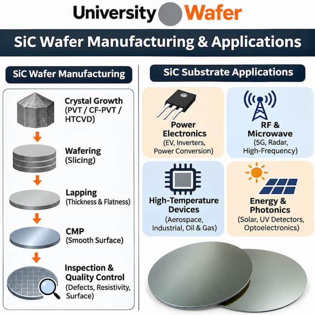
1) Why Use SiC Instead of Silicon?
- Wide bandgap (4H ~3.26 eV): Operates at higher T/V with lower leakage.
- ~10× breakdown field: Thinner drift layers → lower RDS(on), higher efficiency.
- High thermal conductivity (~370 W/m·K): Better heat removal, lighter cooling.
2) SiC Polytypes and Wafer Diameters
4H-SiC dominates power devices; 6H-SiC is used in selected research and optical applications; 3C-SiC remains R&D. Commercial wafer sizes are 100/150 mm with a strong push to 200 mm for capacity and cost structure.
3) SiC Raw Materials and Purification
- Ultra-pure Si & C sources (6N–7N), dopants (N/P for n-type, Al/B for p-type)
- Chemical cleaning (acid leach), thermal conditioning, particle size control
4) SiC Crystal Growth: PVT, CF-PVT and HTCVD
PVT (modified Lely) sublimates high-purity SiC powder & re-crystallizes on a seed (polytype-defining) above 2000 °C in Ar. CF-PVT extends runs with continuous feed (enables larger diameters). HTCVD deposits from gases (silane/propane) with tighter dopant/defect control, at lower growth rates.
5) SiC Ingot Preparation and Wafer Slicing
- Orientation: XRD alignment; 4° off-axis common for 4H epi.
- Shaping: Diamond grinding to target OD, remove outer defects.
- Slicing: Diamond multi-wire; slow to minimize kerf & subsurface damage.
- Edges: Bevel + polish to reduce stress cracks/chipping.
6) SiC Lapping, Polishing and CMP
- Lapping: Remove saw damage, improve parallelism.
- CMP: Diamond/oxidizer slurries; multi-stage finishing can produce very low surface roughness.
- Chemical etch: KOH etching or dry etching can be used to reveal or remove processing damage.
7) SiC Defect Control and Quality Metrology
- Structural: X-ray topography (micropipes, dislocations), EBSD.
- Surface: AFM, optical profilometry, automated optical inspection.
- Electrical: 4-pt resistivity map, Hall (μ, carriers), lifetime (µ-PCD/PL).
- Chemical: SIMS/GDMS for trace elements, dopant profiles.
8) How to Specify SiC Wafers for Your Process
- Choose polytype & off-axis (e.g., 4H, 4° off) aligned with epi requirements.
- Set conductivity (n/p), target resistivity, epi thickness/grade if needed.
- Define diameter, thickness, TTV, bow/warp, and edge profile.
- Call out metrology (AFM RMS, micropipe/dislocation limits, lifetime minimums).
- Packaging/cleanliness: metal-ion & particle specs, certified carriers.
9) SiC Wafer Applications
- Power electronics: EV traction inverters, onboard chargers, DC-DC converters, industrial drives and renewable-energy power conversion.
- RF and microwave: High-power RF devices, radar and communications systems that benefit from thermal stability and high power density.
- Harsh environments: High-temperature sensors and aerospace or industrial systems where conventional silicon may be limiting.
10) SiC Wafer Procurement and Qualification Tips
- Ask for current defect maps and lifetime data with each lot.
- Confirm epi readiness (front CMP target, haze/particles) and edge specs.
- For scaleup: validate 200 mm supply, epi tool compatibility, and carrier/FOUP fit.
Frequently Asked Questions About SiC Wafer Manufacturing
What is the most common SiC polytype for power electronics?
4H-SiC is widely used for power semiconductor devices because its electronic properties and mature epitaxial supply chain support high-voltage and high-temperature device fabrication.
Why is CMP important for silicon carbide wafers?
SiC is extremely hard, so slicing and lapping can leave subsurface damage. Chemical mechanical polishing helps produce a smoother, lower-damage surface suitable for epitaxy and device processing.
Why are off-axis 4H-SiC wafers used for epitaxy?
Off-axis substrates help promote controlled step-flow growth during epitaxy. The required angle depends on the process and wafer specification, so the orientation and off-cut should be defined when ordering.