Silicon Oxide Wafers for Research & Production
Silicon oxide (SiO2) wafers are among the most widely used substrates in
semiconductor fabrication, providing high-quality electrical insulation, surface passivation,
and dielectric isolation for integrated circuits, MEMS, photonic devices, and advanced microelectronics.
Silicon dioxide films may be produced by
thermal oxidation,
wet and dry oxidation,
or CVD deposition,
depending on the desired oxide thickness and device requirements. UniversityWafer supplies
thermal oxide wafers, oxide-coated silicon wafers, and custom SiO2 coatings for
research laboratories, universities, and commercial semiconductor manufacturing.
Silicon Oxide Wafers for Research and Production
UniversityWafer supplies thermal oxide silicon wafers,
deposited SiO2 films, and multilayer dielectric wafers for semiconductor fabrication, MEMS, MOS devices, wafer bonding, photonics, and university research.
Oxide-coated wafers can be supplied with custom wafer diameter, crystal orientation, resistivity, oxide thickness, film uniformity, polish, and single-side or double-side coatings. Additional films such as
silicon nitride,
TEOS oxide, and low-stress LPCVD layers may also be available.
Typical Silicon Oxide Wafer Quote
A researcher from a small technology company requested a custom multilayer wafer configuration for device fabrication:
Requested quantity: 25 wafers
- Wafer diameter: 150 mm
- Conductivity type: N-type, phosphorus-doped
- Crystal orientation: <100>
- Resistivity: 1–10 Ω·cm
- Wafer thickness: 675 ±25 µm
- First film: 10,000 Å ±2% silicon oxide on both sides
- Second film: 8,000 Å ±3% low-stress LPCVD silicon nitride on both sides
- Refractive index: 2.30 ±0.07 at 632.8 nm
- Film stress: Less than 100 MPa
- Surface roughness: Less than 1 nm
Reference number: 270575
This type of silicon oxide and silicon nitride stack may be used for MEMS structures, dielectric isolation, optical devices, passivation layers, masking, and multilayer semiconductor fabrication.
Request a Custom Silicon Oxide Wafer Quote
Tell us the wafer diameter, substrate type, oxide process, film thickness, coating side, quantity, and any required tolerances. Our team can help determine whether
wet or dry thermal oxidation,
CVD oxide, TEOS oxide, or a multilayer dielectric stack is best suited for your process.
Get Your Silicon Oxide Wafer Quote FAST!
Or,
Buy Online
and start researching today.
What Is Silicon Oxide?
Silicon oxide, commonly written as SiO2 and also called silicon dioxide, is a dielectric material composed of silicon and oxygen. In semiconductor processing, it is commonly grown directly on a silicon surface through thermal oxidation or deposited using chemical vapor deposition.
SiO2 provides electrical insulation, surface passivation, chemical stability, and compatibility with lithography, diffusion, etching, and deposition processes. These properties make it important for MOS capacitors, CMOS devices, MEMS, integrated circuits, sensors, photonic structures, and wafer-level research.
Silicon Oxide Wafer Options
-
Thermal Oxide Wafers
— High-quality SiO2 grown directly on silicon.
-
TEOS Oxide Films
— Deposited oxide for conformal coatings and multilayer processing.
-
LPCVD Films
— Controlled dielectric layers for MEMS and semiconductor fabrication.
-
Silicon Nitride on Silicon
— Low-stress and stoichiometric nitride layers for masking, passivation, and membranes.
-
Bare Silicon Wafers
— Available in multiple diameters, orientations, resistivities, and polish options.
-
SOI Wafers
— Silicon device layers separated from the handle wafer by a buried oxide layer.
What Are Silicon Oxide Wafers?
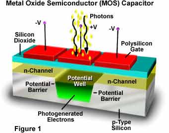 Silicon oxide (SiO2) wafers are among the most widely used substrates in semiconductor manufacturing. A thin layer of silicon dioxide grown or deposited on a silicon wafer provides excellent electrical insulation, surface passivation, diffusion masking, and dielectric isolation for integrated circuits, MEMS devices, photonic components, and sensors.
UniversityWafer supplies thermal oxide wafers, oxide-coated silicon substrates, TEOS oxide wafers, LPCVD oxide films, and custom silicon dioxide thicknesses for university research, semiconductor development, and production applications.
Functions of Silicon Oxide in Semiconductor Fabrication
Silicon dioxide performs several essential functions throughout the IC fabrication process.
Depending on the required device structure, the oxide layer may serve as:
- Gate dielectric for MOS and CMOS devices
- Electrical isolation between conductive layers
- Surface passivation to reduce interface defects
- Diffusion mask during dopant implantation
- Protective layer during wet and dry etching
- Optical dielectric coating for photonic devices
- Sacrificial layer for MEMS fabrication
Thermal Oxide vs CVD Oxide
| Process |
Advantages |
Typical Uses |
| Thermal Oxidation |
Highest interface quality, dense SiO₂, low defect density |
MOS gates, high-performance ICs, MEMS |
| LPCVD / TEOS Oxide |
Excellent thickness control and conformal coverage |
Interlayer dielectrics, MEMS, multilayer devices |
| PECVD Oxide |
Low-temperature deposition |
Temperature-sensitive substrates and back-end processing |
Wet Oxidation vs Dry Oxidation
Both thermal oxidation processes grow silicon dioxide directly from the silicon substrate, but they are optimized for different applications.
| Method |
Characteristics |
Applications |
| Dry Oxidation |
Slower growth, extremely dense oxide, excellent electrical quality |
Gate oxides, MOS capacitors, precision dielectric layers |
| Wet Oxidation |
Much faster growth, ideal for thicker oxide films |
Isolation layers, field oxides, MEMS structures |
Typical Silicon Oxide Thicknesses
| Oxide Thickness |
Common Application |
| 10–100 nm |
Gate oxide and MOS devices |
| 100–500 nm |
Passivation and dielectric isolation |
| 0.5–2 µm |
MEMS fabrication and masking layers |
| 2–10 µm |
Thick oxide structures and specialty research |
Applications of Silicon Oxide Wafers
Silicon oxide coated wafers are used throughout semiconductor manufacturing and advanced research including:
- MEMS fabrication
- MOS capacitors and MOSFET devices
- CMOS integrated circuits
- Photonic integrated circuits
- Microfluidic devices
- Pressure sensors and accelerometers
- Microelectronic packaging
- Wafer bonding
- Advanced semiconductor research
Choosing the Right Silicon Oxide Wafer
Selecting the proper silicon oxide wafer depends on several factors including oxide thickness, deposition method, wafer diameter, crystal orientation, polish, resistivity, and the intended fabrication process. Researchers developing MEMS, photonic devices, CMOS circuits, or power electronics often require different oxide specifications to optimize device performance.
UniversityWafer offers custom oxide thicknesses on
silicon wafers,
SOI wafers,
and specialty semiconductor substrates for research and production quantities.
Frequently Asked Questions
What is the difference between thermal oxide and CVD oxide?
Thermal oxide is grown directly from the silicon wafer, producing a dense, high-quality silicon dioxide layer. CVD oxide is deposited onto the wafer and is commonly used when thicker films or lower processing temperatures are required.
Can silicon oxide thickness be customized?
Yes. Silicon oxide thicknesses can be customized from a few nanometers to several microns depending on the deposition process and research application.
Can I order oxide-coated wafers with silicon nitride?
Yes. UniversityWafer supplies wafers with thermal oxide, LPCVD silicon nitride, TEOS oxide, and other dielectric film combinations used in semiconductor fabrication.
Related Silicon Oxide Products
