
Find Semiconductor Wafers for Your Research
UniversityWafer supplies semiconductor materials and substrates for research, prototyping, and process development. Select the material and wafer specifications according to the device, fabrication process, and equipment you plan to use.
Explore silicon wafers, germanium substrates, gallium arsenide wafers, and silicon carbide substrates. For layered structures, consider silicon-on-insulator (SOI) wafers or epitaxial silicon.
What to Include in a Wafer Quote
- Material, application, and quantity
- Diameter or diced-piece dimensions
- Thickness and acceptable tolerances
- Crystal orientation, conductivity type, and dopant
- Resistivity range and required surface finish
- Oxide, nitride, metal, or epitaxial layers
Get Your Quote Fast! Or Buy Semiconductor Wafers Online and start researching today.
About UniversityWafer
UniversityWafer, Inc. supplies wafers and research substrates. Learn about UniversityWafer or describe your application in the quote form.
Understanding Semiconductor Materials
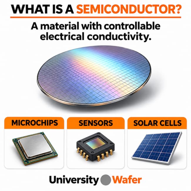
The useful feature of a semiconductor is that its electrical behavior can be engineered. Devices use this control to switch current, amplify signals, detect light, or convert energy.
In this guide: how semiconductors work, intrinsic and doped types, material examples, applications, and manufacturing steps.
Semiconductor vs. Conductor vs. Insulator
These categories describe electrical behavior. Exact conductivity depends on the material and conditions; a semiconductor is not simply a material that conducts “half” as well as a metal.
| Category | Electrical behavior | Examples |
|---|---|---|
| Conductor | Allows current to flow readily | Copper, aluminum |
| Semiconductor | Conductivity can be engineered for device functions | Silicon, germanium, gallium arsenide |
| Insulator | Strongly resists current under ordinary conditions | Glass, silicon dioxide |
How Do Semiconductors Work?
Electrons, holes, and the band gap
Electrons carry negative charge. A hole is a missing electron in an otherwise occupied electronic state and behaves as a positive charge carrier. Both can contribute to current.
The band gap separates the valence and conduction bands. Energy from heat or absorbed light can create mobile electrons and holes. Band structure helps determine which electrical and optical functions a material can support.
Controlling current in a device
Dopants change carrier concentrations, while applied voltages control how carriers move. A field-effect transistor uses an electric field to control a conducting channel. A diode uses a junction or barrier to provide direction-dependent current flow.
Intrinsic and Extrinsic Semiconductors
An intrinsic semiconductor describes the ideal undoped case, where electron and hole concentrations are equal at thermal equilibrium. Extrinsic semiconductors have intentionally introduced dopants that alter the carrier balance.
- N-type: electrons are the majority carriers. Phosphorus is one donor dopant used in silicon.
- P-type: holes are the majority carriers. Boron is one acceptor dopant used in silicon.
Both types remain electrically neutral overall. Semiconductor doping controls carrier concentrations; it does not give the entire wafer a net positive or negative charge. For an order, specify carrier type, dopant if required, and wafer resistivity.
Common Semiconductor Materials and Examples
Silicon and germanium are elemental semiconductors. GaAs, SiC, and GaN are compound semiconductors. Selection depends on the device structure, processing route, and electrical or optical requirements.
| Material | Typical applications |
|---|---|
| Silicon (Si) | Logic and memory chips, MEMS, solar cells |
| Germanium (Ge) | Photodetectors, infrared optics, semiconductor research |
| Gallium arsenide (GaAs) | RF electronics, lasers, optoelectronics |
| Silicon carbide (SiC) | Power conversion and high-temperature device research |
| Gallium nitride (GaN) on sapphire | LEDs and optoelectronic research |
GaN is also used in RF and power devices, but the required substrate and epitaxial stack depend on the application. Compare semiconductor materials before choosing a wafer. SOI is a layered wafer structure, rather than a separate elemental semiconductor.
Why Is Silicon Widely Used?
Silicon supports controlled doping and a mature fabrication ecosystem. It can also form thermal silicon dioxide, an insulating layer used in many processes. Other semiconductors may suit particular optical, high-frequency, or power requirements better.
What Is the Difference Between a Semiconductor, Wafer, and Chip?
- Semiconductor: the material category.
- Wafer: a thin substrate on which devices can be fabricated.
- Die or chip: an individual device or circuit region separated from a processed wafer, often subsequently packaged.
A single wafer can contain many dies. Read what a semiconductor wafer is or see how silicon wafers become computer chips.
What Are Semiconductors Used For?
- Computing and memory: processors, logic, and data storage use large numbers of interconnected transistors.
- Switching and amplification: transistors control electrical signals in circuits.
- Light emission and detection: LEDs generate light, while photodetectors convert incident light into an electrical response.
- Solar energy: solar cells convert light into electrical energy.
- Power conversion: semiconductor switches and diodes control energy in chargers, motor drives, and inverters.
- Sensing: semiconductor devices measure light, temperature, and other physical signals; MEMS devices also incorporate microscopic mechanical structures.
How Are Semiconductor Chips Made?
Blank wafer production comes before device fabrication. For silicon, crystal growth, slicing, polishing, and cleaning produce a substrate. A fabrication facility then builds device structures through repeated processing steps.
- Prepare the wafer: select a clean substrate with appropriate material and geometry.
- Add layers: grow or deposit films needed for the device.
- Pattern and etch: photolithography defines patterns that guide selective material removal or other processing.
- Engineer electrical regions: introduce dopants and apply thermal treatments as required.
- Connect and inspect: form interconnects and check process results.
- Test, separate, and package: evaluate dies, dice the wafer, and assemble devices into suitable packages.
The actual sequence varies by technology. Explore wafer fabrication and integrated circuit fabrication for more detail.
Frequently Asked Questions
Are all semiconductors silicon?
No. Germanium, gallium arsenide, silicon carbide, and gallium nitride are other examples. Different devices need different material properties.
Are all semiconductors single crystals?
No. Semiconductor materials can be single-crystalline, polycrystalline, or amorphous. Many high-performance wafer processes use single-crystal substrates, but that does not define the entire material category.
Does semiconductor resistance always decrease as temperature rises?
No. Temperature affects both carrier concentration and mobility. The resulting resistance depends on doping, temperature range, and material; a simple universal rule is misleading.
What does a semiconductor company do?
Companies may design chips, fabricate them in foundries, combine design and manufacturing, or provide materials, equipment, testing, and packaging. A chip designer does not necessarily own a fabrication plant.
Related Semiconductor Guides
- What is a wafer?
- Silicon wafer doping techniques
- P-type semiconductors
- Silicon wafer resistivity
- Photolithography
- Semiconductor device manufacturing