
What Substrates Are Used for Silicon MEMS Microphones?
Silicon MEMS microphones are commonly fabricated on single-crystal silicon wafers or silicon-on-insulator (SOI) wafers . The preferred substrate depends on the microphone architecture, diaphragm thickness, etching process, electrical requirements, and wafer-level fabrication method.
Standard silicon wafers are widely used for MEMS micromachining because they support mature semiconductor processes such as photolithography, thin-film deposition, wet etching, deep reactive-ion etching (DRIE), oxidation, and wafer bonding.
SOI wafers can be especially useful when a precisely controlled silicon device-layer thickness is required. The buried oxide layer can provide electrical isolation and may also serve as a convenient process-defined etch stop in selected MEMS fabrication flows.
Thin Silicon for Microphone Diaphragms and MEMS Structures
Thin silicon structures are often required inside a MEMS microphone, but that does not necessarily mean the entire starting wafer must be extremely thin. In many fabrication processes, a standard-thickness silicon or SOI wafer is patterned and etched to create the required diaphragm, cavity, backplate, or suspended structure.
For specialized research, however, thin silicon wafers may be useful when reduced substrate thickness is required for handling, transmission, backside processing, mechanical testing, or experimental MEMS structures.
Important parameters can include substrate thickness, device-layer thickness, crystal orientation, resistivity, surface finish, total thickness variation, and wafer flatness.
Why Silicon Is Well Suited to MEMS Microphone Fabrication
Silicon combines well-characterized mechanical properties with mature semiconductor manufacturing technology. This allows microphone structures to be produced with tightly controlled dimensions across many dies on the same wafer.
Benefits of silicon-based MEMS processing include:
- Precise lithographic patterning
- Controlled micrometer-scale structures
- Compatibility with DRIE and anisotropic wet etching
- Wafer-level batch fabrication
- Compatibility with deposited dielectric and conductive films
- Potential integration with CMOS-compatible electronics and packaging
- High repeatability from die to die
These characteristics make silicon an effective substrate platform for capacitive microphones, piezoelectric MEMS microphones, acoustic sensors, microphone arrays, and other microelectromechanical devices.
Silicon Wafer Specifications for MEMS Microphones
Researchers should select the substrate specification according to the required micromachining and device architecture. Useful information to include in a wafer request can include:
- Silicon or SOI wafer type
- Wafer diameter
- Crystal orientation
- Conductivity type
- Resistivity range
- Wafer thickness
- SOI device-layer thickness, if applicable
- Buried oxide thickness
- Handle-wafer thickness
- Single-side or double-side polish
- Surface roughness and flatness requirements
- Required quantity
Get Your Silicon Microphone Substrate Quote FAST! Or, Buy Silicon Wafers Online and Start Researching Today!
How Does a MEMS Microphone Work?
In a common capacitive MEMS microphone, a thin movable diaphragm and a fixed perforated backplate form a miniature variable capacitor. Sound pressure moves the diaphragm, changing the spacing between the two structures and therefore changing the capacitance.
Signal-processing electronics then convert this small capacitance change into a usable analog or digital audio signal. Depending on the package, the MEMS transducer and signal-conditioning ASIC may be fabricated on separate dies and assembled together.
Video: Silicon MEMS Microphones
Applications of Silicon MEMS Microphones
Silicon MEMS microphones are used in compact electronic systems where small size, low power consumption, repeatable performance, and compatibility with semiconductor manufacturing are important.
- Smartphones and tablets
- Laptops and webcams
- Wireless earbuds and headsets
- Hearing aids
- Voice assistants and smart speakers
- Automotive acoustic systems
- Wearable and medical devices
- Microphone arrays and beamforming systems
- Industrial acoustic monitoring
How Silicon MEMS Microphones Work
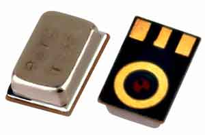
A silicon MEMS microphone is a microfabricated acoustic sensor that converts sound pressure into an electrical signal. In a common capacitive MEMS design, a thin movable diaphragm is positioned near a fixed, perforated backplate. Together, these structures form a variable capacitor.
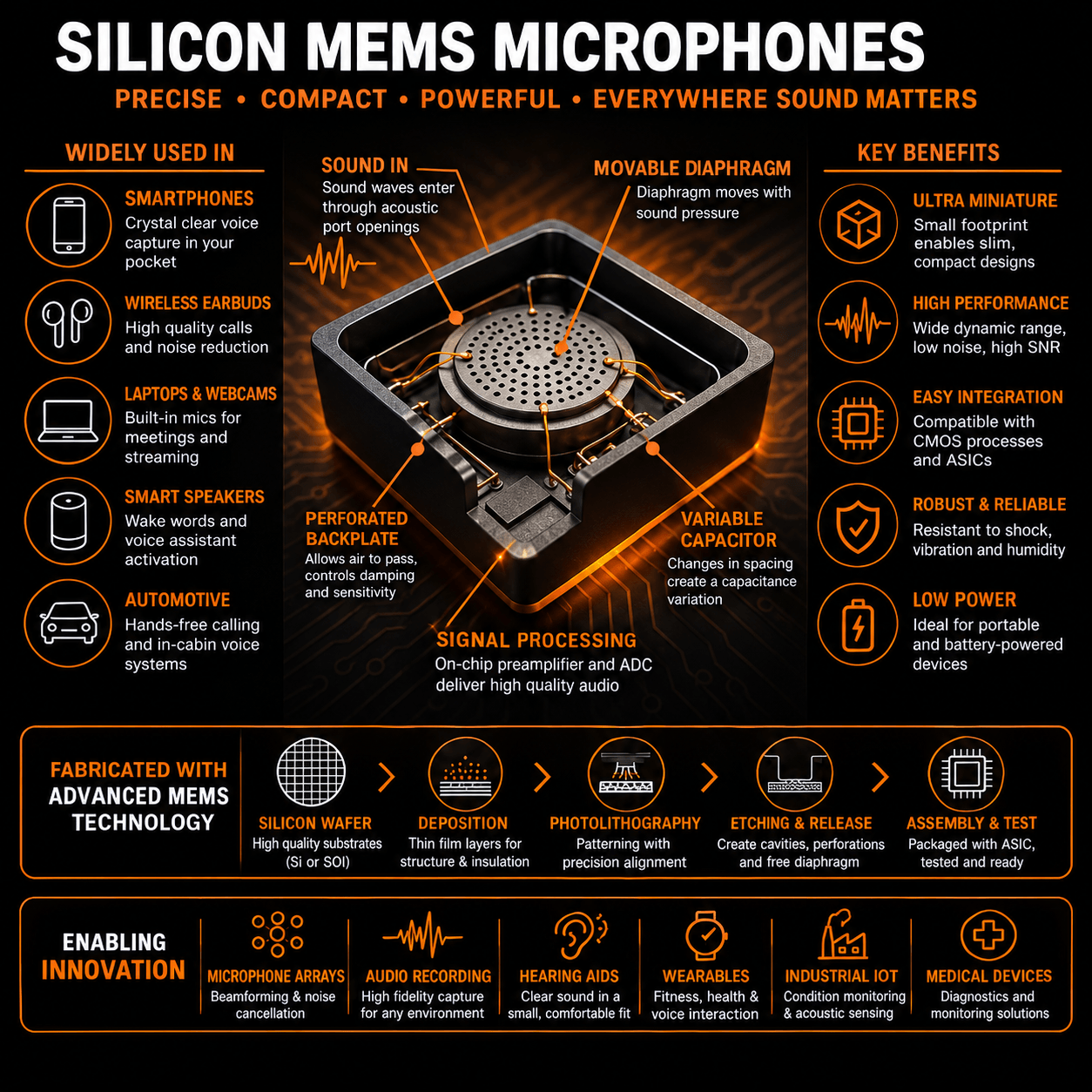
When sound waves enter the microphone package, pressure variations cause the diaphragm to move. This changes the spacing between the diaphragm and backplate and therefore changes the capacitance. The resulting electrical signal can then be amplified and processed by an application-specific integrated circuit (ASIC).
MEMS microphone structures are fabricated using semiconductor-compatible deposition, lithography, etching, and micromachining techniques on silicon wafers or specialized silicon-based substrates.
Why Silicon Is Used for MEMS Microphones
Silicon is well suited to microphone fabrication because it combines predictable mechanical properties with mature semiconductor manufacturing technology. Its compatibility with photolithography, thin-film deposition, dry and wet etching, wafer bonding, and integrated-circuit processing allows very small acoustic structures to be produced with tightly controlled dimensions.
Advantages of silicon-based MEMS microphone fabrication can include:
- Micrometer-scale diaphragm and backplate structures
- High dimensional repeatability across a wafer
- Batch fabrication of many microphone dies simultaneously
- Compatibility with semiconductor packaging and ASIC integration
- Small package size for portable electronics
- Good mechanical stability and repeatable elastic behavior
- Potential for microphone arrays with closely matched sensor elements
Silicon MEMS fabrication is especially useful when large numbers of miniature devices must be produced with consistent mechanical and electrical characteristics.
Silicon Wafer Processing for MEMS Microphones
MEMS microphones are manufactured using combinations of standard semiconductor and micromachining processes. The exact process sequence depends on the microphone architecture, materials, and manufacturer.
Common fabrication steps can include:
- Wafer preparation: A polished silicon or silicon-based substrate is selected according to orientation, thickness, resistivity, and surface requirements.
- Thin-film deposition: Structural, dielectric, conductive, and sacrificial films are formed on the wafer.
- Photolithography: Patterns define the diaphragm, backplate, acoustic openings, contacts, and other MEMS structures.
- Etching: Wet or dry etching removes selected material to create cavities, perforations, and suspended structures.
- Release: Sacrificial material is removed where required so the diaphragm can move in response to acoustic pressure.
- Wafer-level testing and packaging: MEMS dies may be tested, diced, combined with signal-processing electronics, and packaged with an acoustic port.
Bulk Micromachining vs. Surface Micromachining
Silicon microphone structures can be fabricated using bulk micromachining, surface micromachining, or combinations of both.
- Bulk micromachining removes material from the silicon substrate itself to create cavities, membranes, or acoustic openings.
- Surface micromachining builds suspended structures from deposited thin films above the substrate using sacrificial layers that are later removed.
Deep reactive-ion etching (DRIE), anisotropic wet etching, plasma etching, thin-film deposition, and wafer bonding may all be used depending on the microphone design.
Silicon and SOI Wafers for MEMS Microphones
Conventional single-crystal silicon wafers are widely used for MEMS fabrication. Wafer specifications such as crystal orientation, thickness, resistivity, polish, and flatness should be selected according to the intended micromachining process.
Silicon-on-insulator (SOI) wafers can also be useful for MEMS structures because the silicon device layer provides a well-controlled structural thickness while the buried oxide can serve as an electrical isolation layer or process-defined etch stop.
UniversityWafer supplies silicon and SOI substrates for MEMS research with selected diameters, device-layer thicknesses, orientations, resistivities, and surface finishes.
Capacitive MEMS Microphones
Most silicon MEMS microphones use a capacitive transduction principle. A compliant diaphragm and fixed backplate form a miniature capacitor. Sound-induced diaphragm motion changes the capacitance, allowing the acoustic waveform to be converted into an electrical signal.
Backplate perforations allow air to move through the structure and help control acoustic damping. Diaphragm stiffness, air-gap dimensions, perforation geometry, cavity volume, residual stress, and package design all influence microphone sensitivity, bandwidth, noise, and maximum sound pressure level.
Analog vs. Digital MEMS Microphones
The MEMS transducer itself produces a small analog electrical signal that requires signal conditioning. MEMS microphone packages can provide either analog or digital outputs.
- Analog MEMS microphones: The ASIC amplifies and conditions the signal and provides an analog output.
- Digital MEMS microphones: The signal is amplified and converted by an analog-to-digital converter (ADC) before being transmitted through a digital interface.
The MEMS mechanical sensor and signal-conditioning electronics may be fabricated on separate dies and assembled within the same package.
Piezoelectric MEMS Microphones
Although capacitive designs are widely used, MEMS microphones can also use piezoelectric transduction . In a piezoelectric microphone, mechanical strain in a piezoelectric film produces an electrical signal directly.
Piezoelectric MEMS microphone research can involve materials such as AlN, ScAlN, PZT, or other piezoelectric thin films integrated with silicon-based substrates. Their fabrication and electrical architecture differ from conventional capacitive microphone designs.
What Are MEMS Microphones Used For?
MEMS microphones are widely used where compact size, repeatable performance, low power consumption, and compatibility with modern electronics are important.
- Smartphones and tablets
- Laptops and webcams
- Wireless earbuds and headsets
- Hearing aids
- Smart speakers and voice assistants
- Automotive voice and acoustic systems
- Industrial acoustic monitoring
- Medical and wearable electronics
- Microphone arrays and beamforming systems
- Internet-of-Things devices
Modern MEMS microphones are particularly useful in multi-microphone arrays because semiconductor manufacturing can produce sensors with relatively closely matched characteristics, which supports beamforming, noise reduction, and directional audio processing.
MEMS Microphone Performance Parameters
Selecting or designing a MEMS microphone requires more than simply reducing device size. Important acoustic and electrical parameters include:
- Sensitivity
- Signal-to-noise ratio (SNR)
- Equivalent input noise
- Frequency response
- Acoustic overload point
- Total harmonic distortion
- Dynamic range
- Power consumption
- Package and acoustic-port geometry
- Temperature dependence
MEMS geometry, diaphragm properties, backplate design, electronic readout, and package acoustics all contribute to the final performance.
Silicon Microphone Applications in MEMS Research
Silicon microphone research extends beyond consumer audio. MEMS acoustic devices can also be used to investigate miniature pressure sensors, ultrasonic transducers, acoustic resonators, microphone arrays, structural health monitoring, and machine-condition monitoring.
Silicon's compatibility with precision micromachining also enables researchers to study new diaphragm geometries, acoustic cavities, perforated backplates, integrated electronics, wafer-level packaging, and alternative transduction mechanisms.
How to Select Silicon Wafers for MEMS Microphone Fabrication
Researchers fabricating microphone structures should choose the wafer specification according to the intended etching, deposition, bonding, and device-layer requirements.
Important substrate specifications can include:
- Silicon or SOI wafer type
- Wafer diameter
- Crystal orientation
- Device-layer thickness for SOI
- Handle-wafer thickness
- Buried oxide thickness
- Conductivity type and resistivity
- Single-side or double-side polish
- Surface roughness and flatness
- Backside processing requirements
- Required quantity
Silicon wafers and SOI wafers are commonly selected for MEMS because they support precise lithography and micromachining. UniversityWafer's silicon guidance also notes that DSP wafers can be useful when MEMS processing requires backside alignment or etching, while SOI provides a controlled device-layer thickness and buried oxide. :contentReference[oaicite:2]{index=2}