Lithium Niobate (LiNbO3) Wafers for Photonic & Electro-Optic Devices
Lithium Niobate (LiNbO3) wafers are high-performance single-crystal substrates widely used in photonics, electro-optics, telecommunications, nonlinear optics, integrated photonics, and surface acoustic wave (SAW) devices. Their exceptional electro-optic, piezoelectric, and optical properties make them ideal for fabricating optical modulators, waveguides, frequency converters, quantum photonic components, and advanced sensing systems. UniversityWafer supplies custom LiNbO3 wafers with multiple crystal orientations, diameters, thicknesses, and surface finishes to support both research and commercial device fabrication.
Get Your Lithium Niobate Wafer Quote FAST!
UniversityWafer supplies premium Lithium Niobate (LiNbO3) wafers for universities, national laboratories, photonics companies, and semiconductor manufacturers worldwide. Our LiNbO3 substrates support research and production of electro-optic modulators, optical waveguides, integrated photonic circuits, surface acoustic wave (SAW) devices, frequency converters, quantum photonic devices, and advanced optical communication systems.
We offer custom lithium niobate wafers in multiple crystal orientations, diameters, thicknesses, and surface finishes to meet your exact fabrication requirements. Whether you require research quantities or production volumes, our engineering team can recommend the optimal substrate for your application.
LiNbO3 Research Request
A university photonics researcher requested the following custom lithium niobate substrate:
Research Inquiry
We are developing integrated electro-optic modulators for high-speed optical communications using Lithium Niobate (LiNbO3). We are looking for high-quality single-crystal wafers suitable for waveguide fabrication with excellent optical surface quality and tight thickness tolerances.
- Material: Lithium Niobate (LiNbO3)
- Orientation: X-Cut
- Diameter: 4 inch (100 mm)
- Thickness: 500 µm
- Surface Finish: Double-side polished
- Application: Electro-optic waveguide fabrication
- Quantity: Prototype research lot
Information to Include With Your Quote Request
To help our engineers recommend the best lithium niobate wafer, please include as many specifications as possible:
- Crystal orientation (X-Cut, Y-Cut, Z-Cut, etc.)
- Wafer diameter
- Wafer thickness
- Single-side or double-side polished
- Surface quality requirements
- Edge profile
- Application (SAW, photonics, modulators, PPLN, etc.)
- Quantity required
Get Your Lithium Niobate Wafer Quote FAST! Or,
Buy Online and Start Researching Today!
Typical Lithium Niobate Wafer Options
- X-Cut, Y-Cut, Z-Cut, and custom crystal orientations
- 2", 3", 4", and 6" wafer diameters
- Single-side and double-side polished surfaces
- Optical-grade surface finishes
- Custom thicknesses and edge profiles
- Thin-Film Lithium Niobate (TFLN) and LNOI substrates
- Research, pilot production, and commercial quantities
What Are Lithium Niobate Wafers?
Lithium Niobate (LiNbO3) wafers are single-crystal substrates valued for their exceptional electro-optic, piezoelectric, pyroelectric, and nonlinear optical properties. These characteristics make lithium niobate one of the most widely used materials for fabricating optical modulators, waveguides, frequency converters, surface acoustic wave (SAW) devices, and integrated photonic circuits.
UniversityWafer supplies high-quality LiNbO3 wafers for university research, government laboratories, and commercial semiconductor and photonics applications. Standard and custom specifications are available to support both prototype development and production.
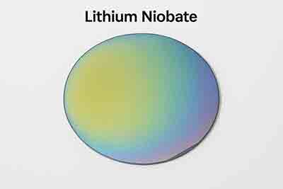
Key Properties of LiNbO3
Lithium niobate combines excellent optical transparency with outstanding electro-optic performance, making it ideal for high-speed optical communication systems and precision sensing technologies.
- Excellent electro-optic coefficient
- High optical transparency from visible to infrared wavelengths
- Strong nonlinear optical response
- Piezoelectric and pyroelectric properties
- Low optical loss for waveguide fabrication
- High chemical and thermal stability
- Excellent frequency conversion efficiency
Available Wafer Orientations
Different crystal orientations provide unique electrical and optical characteristics depending on the intended application.
- X-Cut Lithium Niobate – Frequently used for electro-optic modulators and integrated photonics.
- Y-Cut Lithium Niobate – Common for acousto-optic and surface acoustic wave (SAW) devices.
- Z-Cut Lithium Niobate – Ideal for nonlinear optics, optical waveguides, and frequency conversion.
- Custom crystal orientations available upon request.
Applications of Lithium Niobate Wafers
Researchers and manufacturers use LiNbO3 substrates across a broad range of photonic and electronic technologies, including:
- Electro-optic modulators
- Integrated photonic circuits
- Optical waveguides
- Fiber optic communication systems
- Surface Acoustic Wave (SAW) devices
- Acousto-optic modulators
- Frequency doublers and second-harmonic generation (SHG)
- Periodically Poled Lithium Niobate (PPLN) devices
- Quantum photonics
- Laser systems
- Optical sensors
- Telecommunications
Custom Lithium Niobate Wafer Specifications
UniversityWafer offers custom lithium niobate wafers with a variety of diameters, thicknesses, crystal orientations, surface finishes, edge profiles, and polishing options. We also provide substrates for advanced Lithium Niobate on Insulator (LNOI) and thin-film lithium niobate research to support next-generation integrated photonic devices.
Why Researchers Choose Lithium Niobate
Compared with many optical materials, lithium niobate offers an excellent combination of optical transparency, fast electro-optic response, nonlinear optical efficiency, and long-term stability. These advantages have made it one of the most important substrate materials for modern photonics, quantum technologies, microwave photonics, and optical communication systems.
Related Resources
