
Tell Us About Your Research Needs
Whether you are developing MEMS devices, fabricating microelectronic components, testing thin-film coatings, or characterizing new semiconductor materials, UniversityWafer, Inc. can supply the research-grade wafers and substrates needed for reliable experimental results.
We provide silicon, sapphire, quartz, fused silica, SOI, silicon carbide, gallium arsenide, gallium nitride, germanium, indium phosphide, and other advanced materials for semiconductor research, photonics, optoelectronics, nanofabrication, quantum devices, materials science, and sensor development.
Tell us your required wafer material, diameter, crystal orientation, dopant type, resistivity, thickness, surface finish, coating, and quantity. Our team will respond with pricing, lead time, and current availability tailored to your research project.
Get Your Research Wafer Quote FAST! Or, Buy Online and Start Researching Today!
Quick Wafer Specification Guide
Providing complete wafer specifications helps us identify the most appropriate in-stock or custom substrate for your application.
- Material: Silicon, sapphire, SOI, SiC, GaAs, GaN, InP, germanium, quartz, fused silica, or another specialty substrate
- Diameter: Small research samples through 300 mm wafers
- Crystal orientation: <100>, <110>, <111>, C-plane, A-plane, or R-plane
- Dopant type: P-type, N-type, intrinsic, semi-insulating, or undoped
- Resistivity: Low-, medium-, or high-resistivity material
- Thickness: Standard or custom wafer thickness
- Dimensional tolerances: Total thickness variation (TTV), bow, warp, flatness, and edge profile
- Surface finish: Single-side polished (SSP), double-side polished (DSP), etched, lapped, or as-cut
- Thin-film coatings: Thermal oxide, silicon nitride, metals, epitaxial layers, or custom deposited films
- Quantity: Individual research wafers, small R&D lots, or pilot-production quantities
- Delivery requirements: Desired lead time, packaging, and shipping destination
Send Your Wafer Specifications
Custom Wafer Processing Services
UniversityWafer can support research and development projects with value-added wafer-processing services, including:
- Thermal oxidation and precision SiO₂ coatings
- LPCVD and PECVD silicon nitride and dielectric coatings
- Wafer thinning and back-grinding
- Single-side and double-side polishing
- Wafer dicing and custom-cut substrates
- Metal deposition and metallization
- Wafer bonding and multi-material integration
- Epitaxial growth and specialty thin films
- Cleanroom packaging and particle-controlled handling
Research Quantities and Lead Times
In-stock semiconductor wafers and dielectric substrates can often ship quickly. Custom wafer orders depend on material availability, processing requirements, coating thickness, dimensional tolerances, and quantity.
We support individual wafer purchases, university research projects, laboratory testing, prototype fabrication, R&D lots, and pilot-production runs. Small quantities allow researchers to evaluate a material or process before committing to larger orders.
Research-Grade Semiconductor Substrates for Advanced R&D
UniversityWafer, Inc. supplies research-grade semiconductor substrates and dielectric wafers that support cutting-edge research in microelectronics, materials science, nanotechnology, photonics, optoelectronics, MEMS fabrication, quantum computing, and semiconductor device development. Our portfolio includes precision silicon wafers, sapphire wafers, and compound semiconductor wafers such as silicon carbide (SiC), gallium arsenide (GaAs), gallium nitride (GaN), and indium phosphide (InP). Every substrate is manufactured for exceptional flatness, cleanliness, low defect density, and reproducibility, making them ideal for university laboratories, government research facilities, and commercial R&D organizations worldwide.
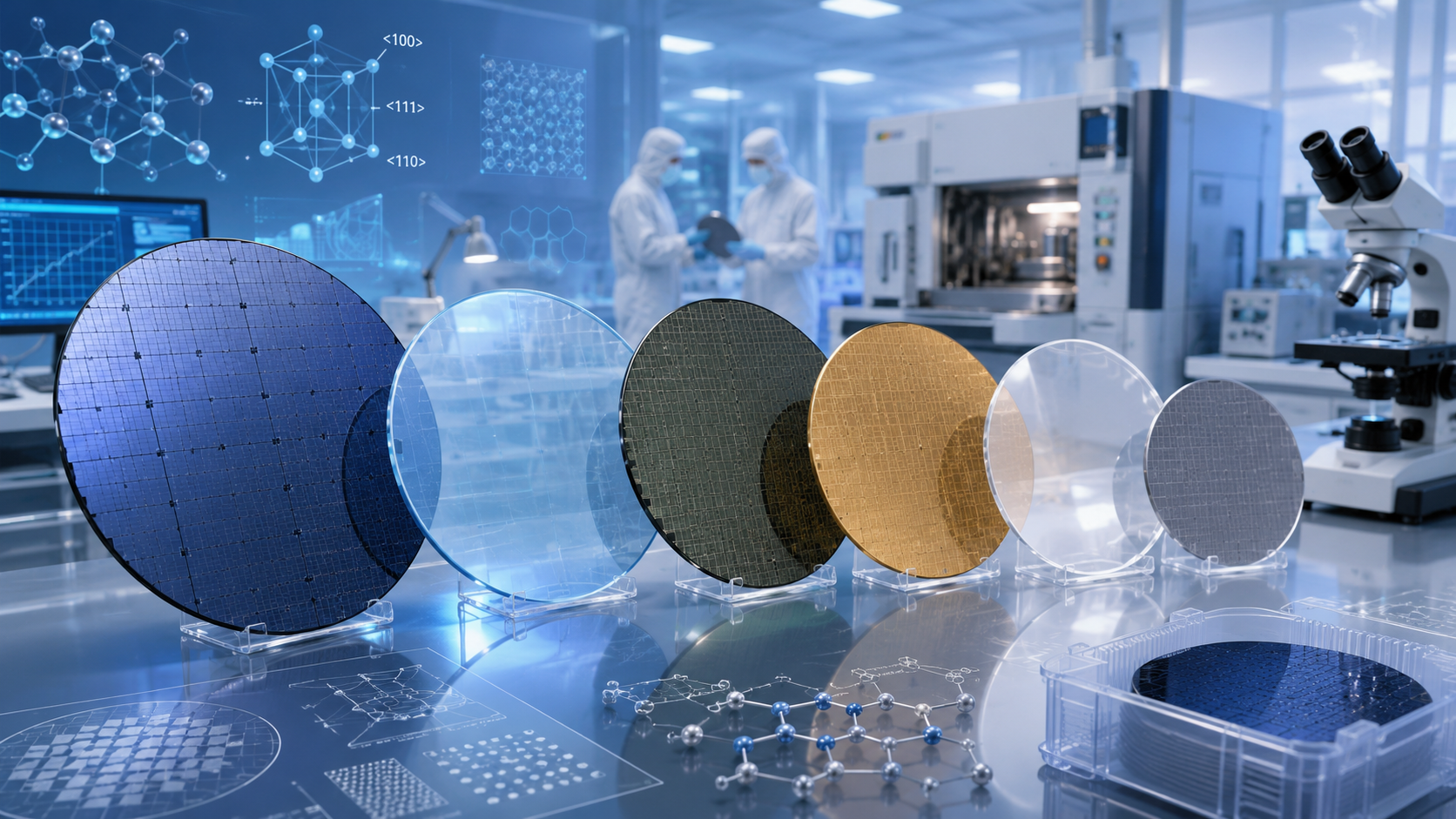
Supporting Innovation Across Semiconductor Research
Researchers rely on UniversityWafer substrates throughout the semiconductor fabrication process—from wafer preparation and thin-film deposition to lithography, etching, wafer bonding, device characterization, and prototype manufacturing. Whether developing MEMS sensors, photonic integrated circuits, quantum devices, RF electronics, power semiconductors, or advanced coating materials, our wafers provide the dimensional accuracy and material consistency required for repeatable experimental results.
- Microelectronics: Prime grade and test grade silicon wafers for process calibration and prototype fabrication.
- Photonics and Optoelectronics: Sapphire, GaN-on-Si, and quartz wafers for high optical transmission and heat stability.
- MEMS and Sensors: SOI and single-crystal silicon substrates with minimal bow and total thickness variation (TTV).
- Quantum and Cryogenic Research: Ultra-flat, high-resistivity silicon and fused silica wafers for superconducting and spin-based systems.
- Energy and Materials Science: SiC, GaAs, and Ge wafers for solar, thermoelectric, and high-power experiments.
Precision and Customization
Every research project demands specific characteristics. UniversityWafer provides custom wafer specifications—including diameter, orientation, dopant type, resistivity, and surface polish—to match each application. We regularly supply wafers with RMS roughness under 10 Å for AFM and profilometer measurements, and thermal oxide layers tuned for dielectric and stress testing.
Our engineers also prepare custom-cut substrates and thin samples for optical, mechanical, and deposition studies, enabling precise experimental control and reproducible results.
Common Research-Grade Options
- Silicon wafers: 2–300 mm diameters, <100> and <111> orientations, P-type or N-type doping
- Sapphire: C-plane, A-plane, and R-plane, double-side polished for optical testing
- GaN-on-Si and SiC substrates for high-power and RF research
- Oxidized silicon wafers with SiO₂ layers from 10 nm to 5 µm
- Fused silica and quartz for AFM, profilometry, and surface characterization
Collaboration with Academia and Industry
UniversityWafer collaborates with universities, government laboratories, and commercial research centers in more than 100 countries. Beyond material supply, our goal is to bridge academic innovation with industrial scalability. Researchers benefit from small-lot quantities, fast delivery, and competitive pricing designed to support experimentation and pilot production.
Real-World Results
From thin-film stress measurements using profilometers to microfluidic devices patterned on SOI wafers, our materials improve the precision and consistency of laboratory outcomes. High-quality surfaces, low defect densities, and controlled doping enable reliable signal performance, stable mechanical properties, and greater device yield during fabrication.
Research Areas We Support
| Field | Substrate Example | Application |
| MEMS and Actuators | SOI, SiN-coated Si | Micro-devices, sensors, and precision motion structures |
| Photonics | Sapphire, Quartz | Optical waveguides, mirrors, and LED wafer templates |
| Quantum Devices | High-resistivity Si, GaAs | Superconducting qubits, quantum dots, cryogenic systems |
| Thin-Film and Coating Studies | Oxidized Silicon, Fused Silica | Film stress analysis, adhesion, and deposition calibration |
| Energy Systems | SiC, GaN, Ge | Power electronics, photovoltaics, thermoelectric research |
Accelerating Discovery
By delivering reliable, affordable, and research-grade wafers, UniversityWafer shortens the path between concept and demonstration. Our substrates give researchers the stability and repeatability needed to publish faster, prototype efficiently, and scale emerging technologies.
Related Research Resources
- Silicon Wafers – Research-grade silicon substrates for microelectronics, MEMS, sensors, and semiconductor fabrication.
- Silicon Substrates – Learn how silicon substrates are used in semiconductor device development and thin-film research.
- Semiconductor Materials – Compare silicon, GaAs, SiC, GaN, germanium, and other semiconductor materials.
- Photonic Devices – Semiconductor substrates for photonics, integrated optics, and optical communications.
- MEMS Research – Silicon, SOI, and specialty wafers for microelectromechanical systems.
- Silicon-on-Insulator (SOI) Wafers – Ideal substrates for MEMS fabrication, RF electronics, and low-power devices.
- Silicon Carbide (SiC) Wafers – Wide-bandgap semiconductor substrates for power electronics and high-temperature applications.
- Gallium Nitride (GaN) Wafers – GaN substrates for RF devices, LEDs, and high-frequency electronics.
- Gallium Arsenide (GaAs) Wafers – Compound semiconductor substrates for photonics, microwave devices, and solar cells.
- Indium Phosphide (InP) Wafers – High-speed optoelectronic and photonic device substrates.
- Germanium Wafers – Infrared optics, photodetectors, and advanced semiconductor research.
- Thermal Oxide Wafers – Silicon wafers with precision SiO₂ layers for dielectric isolation and device fabrication.
- Silicon Nitride Wafers – LPCVD and PECVD silicon nitride coatings for MEMS, passivation, and etch-mask applications.
- Quartz Wafers – High-purity quartz substrates for photonics, optics, and precision measurement applications.
- Fused Silica Wafers – Ultra-low thermal expansion substrates for optical and scientific research.