
What Is the Difference Between Amorphous and Crystalline Solids?
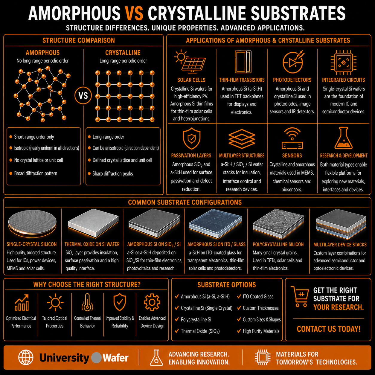
The primary difference between amorphous and crystalline solids is the way their atoms, ions, or molecules are arranged. In a crystalline material, the constituent particles exhibit long-range structural order. Their arrangement follows an ordered crystal structure that extends over large distances within a crystal.
An amorphous material, by contrast, does not possess the same long-range periodic crystal structure. The atoms can still exhibit short-range order, meaning neighboring atoms maintain characteristic bonding distances and local arrangements, but this order does not repeat periodically throughout the material.
This difference in atomic organization can strongly influence a material's electrical, optical, thermal, and mechanical properties. It is particularly important in semiconductor research, where both crystalline and amorphous materials can be deliberately incorporated into thin films and device structures.
What Is a Crystalline Solid?
A crystalline solid contains an ordered atomic arrangement characterized by long-range structural order. In conventional crystals, this structure can be described using a repeating unit cell, which represents the fundamental repeating arrangement of atoms within the crystal lattice.
Semiconductor wafers made from materials such as single-crystal silicon , germanium, gallium arsenide, silicon carbide, and sapphire rely on well-defined crystalline structures.
Crystal orientation is therefore an important wafer specification. For example, silicon wafers are commonly supplied with orientations such as (100) and (111). Orientation can affect processes and properties including anisotropic etching, oxidation behavior, surface atomic structure, epitaxial growth, and device fabrication.
What Is an Amorphous Solid?
An amorphous solid is a non-crystalline solid that lacks the long-range periodic atomic order found in a crystal. This does not mean that its atoms are completely random. Local bonding and short-range structural order can still exist.
Common examples of materials that can occur in amorphous form include glasses, polymers, metallic glasses, amorphous silicon, and many thin-film materials.
It is sometimes stated that amorphous solids are simply supercooled liquids. That description can be misleading when used as a general definition. Glass formation can involve cooling a liquid without crystallization, but an amorphous solid is mechanically a solid and is more accurately distinguished from a crystalline material by its lack of long-range crystalline order.
Amorphous vs. Crystalline Structure
| Property | Crystalline Solid | Amorphous Solid |
|---|---|---|
| Atomic Arrangement | Long-range structural order | No long-range periodic crystalline order |
| Short-Range Order | Present | Generally present to varying degrees |
| Crystal Lattice | Defined crystalline structure | No periodic crystal lattice |
| Unit Cell | Can describe the repeating crystal structure | No repeating crystallographic unit cell describing the entire structure |
| Diffraction | Typically produces distinct diffraction peaks | Typically produces broad diffuse scattering rather than sharp crystal peaks |
| Thermal Behavior | Crystalline phases can exhibit a well-defined melting transition | Glasses typically soften through a glass-transition region before viscous flow |
| Directional Properties | Can be anisotropic | Often approximately isotropic on a macroscopic scale |
| Semiconductor Example | Single-crystal silicon (c-Si) | Amorphous silicon (a-Si or a-Si:H) |
Amorphous Silicon vs. Crystalline Silicon
The difference between amorphous and crystalline structure is especially important in silicon semiconductor materials.
Crystalline silicon (c-Si) has a highly ordered diamond-cubic crystal structure. Single-crystal silicon wafers are widely used for integrated circuits, MEMS, sensors, power devices, photovoltaics, and many other semiconductor applications.
Amorphous silicon (a-Si) lacks the long-range crystalline order of c-Si. Although local silicon bonding retains some short-range structural organization, disorder in the network can create defects, including dangling bonds, that strongly influence electronic properties.
Hydrogen is commonly incorporated to form hydrogenated amorphous silicon (a-Si:H). Hydrogen can passivate many dangling bonds and reduce electrically active defect states, improving the material's usefulness in electronic and photovoltaic applications.
Why Does Crystal Structure Matter in Semiconductors?
Atomic structure influences how charge carriers and light interact with a semiconductor. Changing a material from an ordered crystalline structure to a disordered amorphous structure can change its electronic density of states, carrier transport, optical absorption, defect population, and other material properties.
This does not mean that crystalline materials are always superior. Crystalline and amorphous materials are useful for different purposes. Device engineers select the appropriate material according to the electrical, optical, thermal, mechanical, and processing requirements of the application.
Why Is Amorphous Silicon Used?
Amorphous silicon is useful because it can be deposited as a thin film rather than requiring the growth and slicing of a bulk single crystal. This allows silicon-containing device layers to be formed on suitable supporting substrates.
Depending on the deposition process and device requirements, amorphous silicon films can be incorporated into:
- Thin-film photovoltaic devices
- Silicon heterojunction solar cells
- Thin-film transistors
- Photodetectors and photosensors
- Research thin-film structures
- Passivation and semiconductor interface structures
Get Your Substrate Quote FAST! Or, Buy Wafers Online and Start Researching Today!
Amorphous Silicon Thin Films on Silicon Wafers
Researchers may also deposit amorphous silicon onto crystalline silicon wafers or onto wafers containing dielectric layers such as SiO2.
This creates a structure in which an amorphous semiconductor film and a crystalline substrate are intentionally combined in the same research sample. The properties of the structure can be tailored through film thickness, hydrogen content, doping, deposition conditions, substrate preparation, and post-deposition processing.
How Are Amorphous and Crystalline Materials Identified?
Researchers use several characterization methods to investigate whether a material is crystalline, amorphous, or contains a mixture of structural phases.
- X-ray diffraction (XRD): Crystalline materials typically produce distinct diffraction peaks, while amorphous materials generally produce broader diffuse features.
- Raman spectroscopy: Can distinguish changes in bonding and structural order in materials such as silicon.
- Transmission electron microscopy (TEM): Can directly investigate atomic-scale structure and crystalline regions.
- Electron diffraction: Provides information about crystallographic order and orientation.
- Spectroscopic ellipsometry: Can help characterize optical properties, film thickness, and structural changes in semiconductor thin films.
Amorphous, Polycrystalline, and Single-Crystal Materials
Semiconductor materials are not limited to only amorphous and single-crystal structures. Polycrystalline materials contain many individual crystalline grains separated by grain boundaries.
- Single crystal: Long-range crystal order extends continuously through the crystal without grain boundaries.
- Polycrystalline: Contains multiple crystalline grains with different crystallographic orientations.
- Amorphous: Does not exhibit the long-range periodic order characteristic of a crystalline lattice.
Distinguishing among these structures is important because grain boundaries, structural disorder, defects, and interfaces can substantially affect semiconductor performance.
Applications of Amorphous and Crystalline Silicon
Both material forms are important in semiconductor and materials-science research, but they are selected for different reasons.
- Crystalline silicon: integrated circuits, MEMS, power electronics, sensors, photovoltaics, photonics, and semiconductor research
- Amorphous silicon: thin-film devices, photovoltaic structures, thin-film transistors, photodetectors, passivation layers, and materials research
- Combined amorphous/crystalline structures: heterojunction devices, interface studies, passivation research, and experimental semiconductor structures
How Atomic Structure Affects Material Properties
The difference between amorphous and crystalline materials is more than a visual difference in atomic arrangement. Structural order influences electronic states, charge transport, optical response, mechanical behavior, thermal transport, and the way a material interacts with other layers in a device.
In a crystalline semiconductor, long-range atomic order creates a well-defined periodic potential for electrons. In an amorphous semiconductor, structural disorder modifies the electronic structure and can introduce localized electronic states associated with disorder and defects.
As a result, two materials with the same chemical composition can exhibit substantially different properties depending on whether they are single-crystal, polycrystalline, or amorphous.
Electrical Properties: Amorphous vs. Crystalline Silicon
Crystalline silicon (c-Si) has a periodic diamond-cubic crystal structure and generally supports substantially higher carrier mobility than amorphous silicon. This is one reason single-crystal silicon wafers are widely used for integrated circuits and other high-performance semiconductor devices.
Amorphous silicon (a-Si) lacks long-range crystalline order. Structural disorder and defects can produce localized electronic states and reduce carrier mobility compared with high-quality single-crystal silicon.
These differences do not make amorphous silicon unsuitable for electronic devices. Instead, a-Si and hydrogenated amorphous silicon (a-Si:H) are useful when thin-film deposition, large-area processing, optical absorption, passivation, or other application-specific properties are more important than achieving the carrier mobility of single-crystal silicon.
Why Is Hydrogen Added to Amorphous Silicon?
The disordered atomic network of amorphous silicon can contain dangling bonds and other defect states that affect its electronic properties. Incorporating hydrogen during deposition produces hydrogenated amorphous silicon (a-Si:H).
Hydrogen can passivate many silicon dangling bonds, reducing the density of electrically active defect states. This improves the usefulness of amorphous silicon in electronic, photovoltaic, photodetector, and passivation applications.
Optical Properties of Amorphous and Crystalline Silicon
Structural order also affects how silicon interacts with light. Crystalline silicon is an indirect-band-gap semiconductor, which influences its optical absorption near the band edge.
Amorphous silicon does not have the same well-defined crystal momentum relationships because it lacks long-range periodic order. Its electronic and optical behavior is broadened by structural disorder, and hydrogenated amorphous silicon can exhibit strong optical absorption over useful portions of the solar spectrum.
This is one reason relatively thin a-Si:H absorber layers can be used in certain thin-film photovoltaic and photosensitive devices.
Thermal Behavior of Amorphous vs. Crystalline Solids
Crystalline and amorphous materials can also differ in their thermal transitions. A crystalline phase can undergo a well-defined melting transition at its equilibrium melting temperature under a specified pressure.
Glass-forming amorphous materials instead exhibit a glass-transition region, where their mechanical response and molecular or atomic mobility change progressively with temperature. They can subsequently soften and flow without undergoing the same first-order melting transition characteristic of a corresponding crystalline phase.
The exact behavior depends strongly on material composition, heating rate, processing history, and structure, so the simple statement that “crystalline solids melt while amorphous solids do not” should be avoided.
Are Amorphous Materials Always Isotropic?
Amorphous materials are often described as isotropic because they lack a macroscopic crystallographic orientation. In an ideal, homogeneous amorphous material, many properties can therefore be similar in different directions.
However, amorphous materials should not automatically be assumed to be perfectly isotropic. Deposition conditions, residual stress, interfaces, molecular alignment, composition gradients, and processing can introduce directional behavior.
Crystalline materials, in contrast, can exhibit anisotropic properties because their atomic arrangement depends on crystallographic direction.
Crystal Orientation in Silicon Wafers
The directional properties of crystalline materials are particularly important in semiconductor wafer processing. Single-crystal silicon substrates are commonly specified by crystallographic orientation, such as Si(100) or Si(111).
Orientation can influence surface structure, anisotropic etching, epitaxial growth, interface formation, mechanical behavior, and certain device fabrication processes.
This is why silicon wafer orientation is an important substrate specification, while an amorphous film does not have a conventional Miller-index crystal orientation.
How Are Amorphous Silicon Films Deposited?
Unlike bulk single-crystal silicon wafers, amorphous silicon is commonly produced as a deposited thin film. Deposition conditions are selected to form a non-crystalline silicon layer and control properties such as thickness, hydrogen incorporation, doping, stress, and defect density.
Hydrogenated amorphous silicon is commonly deposited using plasma-enhanced chemical vapor deposition (PECVD). Other deposition techniques may also be used depending on the desired material and research application.
The supporting substrate can be crystalline silicon, oxidized silicon, glass, or another material compatible with the deposition process.
Amorphous Silicon on SiO2/Silicon Wafers
Researchers frequently investigate multilayer structures that combine amorphous and crystalline materials. One example is:
a-Si:H → SiO2 → Crystalline Silicon Wafer
In this structure, the underlying crystalline silicon wafer provides mechanical support and a well-defined semiconductor substrate. The SiO2 layer can provide electrical isolation, surface passivation, or a controlled dielectric interface, while the amorphous silicon layer provides the functional thin-film semiconductor.
Researchers can vary oxide thickness, amorphous-silicon thickness, hydrogen content, doping, substrate resistivity, and thermal processing to study interfaces and device behavior.
Amorphous Silicon on ITO and Transparent Substrates
Amorphous silicon can also be incorporated into structures containing transparent conductive oxides such as indium tin oxide (ITO) .
Transparent conductive layers provide a combination of optical transmission and electrical conductivity, making them useful in photovoltaic, photodetector, sensor, and experimental optoelectronic structures.
When designing an a-Si:H/TCO structure, researchers should consider substrate temperature, film adhesion, interface quality, sheet resistance, optical transmission, surface roughness, and compatibility with subsequent processing.
Amorphous and Crystalline Silicon in Solar Cells
Both amorphous and crystalline silicon are important photovoltaic materials, but they are used differently.
Crystalline silicon is the dominant absorber material in conventional silicon photovoltaic cells. High-quality crystalline wafers provide efficient carrier transport and long carrier lifetimes when appropriately processed.
Hydrogenated amorphous silicon can be deposited in thin layers and has been used in thin-film photovoltaic devices. It is also technologically important in silicon heterojunction solar cells, where thin amorphous-silicon-based layers are combined with a crystalline silicon wafer.
These heterostructures demonstrate that amorphous and crystalline materials do not need to be competing alternatives; they can be combined to exploit different material properties within the same device.
Amorphous vs. Crystalline vs. Polycrystalline Silicon
| Property | Amorphous Silicon | Polycrystalline Silicon | Single-Crystal Silicon |
|---|---|---|---|
| Long-Range Order | Absent | Present within individual grains | Present throughout the single crystal |
| Grain Boundaries | No conventional crystalline grains | Present | Absent within an ideal single crystal |
| Crystal Orientation | No single crystallographic orientation | Varies among grains | Defined wafer orientation |
| Typical Form | Deposited thin film | Thin film or bulk material | Wafer or epitaxial layer |
| Carrier Transport | Strongly affected by disorder and localized states | Affected by grains and grain boundaries | Generally highest quality when defects and impurities are well controlled |
| Example Applications | Thin-film devices, passivation, photovoltaics | Solar cells, gates, thin-film electronics | ICs, MEMS, power devices, sensors, photovoltaics |
Applications of Amorphous Materials in Semiconductor Research
Amorphous materials are important throughout semiconductor processing, not only as active semiconductor layers. Amorphous thin films can provide electrical isolation, passivation, optical functionality, protective coatings, and precursor layers for later crystallization.
Examples include:
- Hydrogenated amorphous silicon (a-Si:H)
- Amorphous silicon dioxide (SiO2)
- Amorphous dielectric thin films
- Thin-film transistor structures
- Photovoltaic absorber and passivation layers
- Optical coatings
- Semiconductor interface research
- Thin-film materials characterization
Applications of Crystalline Semiconductor Materials
Crystalline semiconductor substrates are preferred when devices require controlled crystal orientation, high-quality carrier transport, reproducible electronic properties, epitaxial compatibility, or precise semiconductor fabrication.
Common applications include:
- Integrated circuits and CMOS devices
- MEMS sensors and actuators
- Power semiconductor devices
- Photodetectors
- Crystalline silicon solar cells
- Silicon photonics
- Epitaxial semiconductor growth
- Quantum and advanced materials research
Choosing a Substrate for Amorphous Thin-Film Research
When ordering substrates for amorphous thin-film deposition, researchers should consider both the properties of the deposited film and the underlying substrate.
Useful specifications can include:
- Substrate material
- Wafer or sample dimensions
- Crystal orientation, when applicable
- Conductivity type and resistivity
- Surface finish and roughness
- Thermal oxide thickness
- Transparent conductive coating, if required
- Amorphous film composition
- Film thickness
- Doping requirements
- Hydrogenation requirements
- Maximum processing temperature
- Required quantity