
Choosing Glass Wafers for Research and Fabrication
Glass wafers are used as transparent, electrically insulating, and chemically stable substrates in MEMS, microfluidics, optics, photonics, sensors, displays, and semiconductor research. Unlike crystalline silicon wafers, most technical glasses are amorphous and do not have the crystallographic orientation requirements associated with crystalline substrates.
Selecting the right glass substrate depends on the application. Important factors include glass composition, optical transmission, coefficient of thermal expansion (CTE), thickness, surface polish, flatness, chemical resistance, and bonding compatibility.
UniversityWafer supplies glass substrates for research, development, prototyping, and specialized fabrication, including borosilicate, fused silica, D263, BK7, Corning glass, soda-lime, and other specialty glass materials.
What Glass Wafer Specifications Should You Choose?
When requesting glass wafers, consider both the material and the physical specifications required by your fabrication process. Providing these details can help identify the most suitable substrate for your experiment.
Glass Material
Different glass compositions provide different optical, thermal, electrical, and chemical properties.
- Borosilicate: Commonly selected for MEMS, microfluidics, sensors, and silicon-to-glass anodic bonding.
- Fused Silica : Useful for UV optics, photonics, spectroscopy, laser applications, and processes requiring very low thermal expansion.
- D263 Glass : Thin specialty glass used in displays, micro-optics, sensors, and thin-film devices.
- BK7 Glass : Common optical glass for imaging, photonics, spectroscopy, and optical research.
- Soda-Lime Glass : A cost-effective option for general testing, displays, windows, and prototype applications.
Wafer Diameter and Thickness
Glass wafers can be supplied in standard semiconductor-style diameters as well as custom dimensions. Thickness should be selected based on mechanical strength, optical path length, device geometry, handling, and bonding requirements.
Thin and ultra-thin glass can be useful for compact optical devices, displays, sensors, flexible-device research, and applications where reduced substrate thickness is important.
Surface Polish and Roughness
Surface quality can be especially important for photolithography, optical devices, thin-film deposition, microfluidics, and wafer bonding. Depending on the application, researchers may require single-side polished (SSP), double-side polished (DSP), or optical-quality surfaces.
Double-side polished glass is particularly useful when optical access, processing, alignment, or bonding is required on both surfaces.
Flatness, Bow, Warp and TTV
Precision fabrication can require control of wafer flatness, bow, warp, and total thickness variation (TTV) . These parameters become especially important during lithography, wafer bonding, coating, and precision alignment.
Optical Properties of Glass Wafers
Optical transmission varies significantly between glass materials. Fused silica is frequently selected for UV and optical applications, while borosilicate, BK7, D263, and other specialty glasses can be selected according to the wavelength range and optical performance required by the device.
Important optical specifications may include:
- Transmission wavelength range
- Refractive index
- Surface roughness and polish quality
- Absorption
- Internal stress and birefringence
- Anti-reflective or other optical coatings
Thermal Properties and CTE
The coefficient of thermal expansion (CTE) is an important consideration when glass is bonded to silicon, metals, or other materials. A large thermal-expansion mismatch can introduce mechanical stress during heating and cooling.
Fused silica has particularly low thermal expansion, while selected borosilicate glasses provide thermal properties that make them useful for silicon-to-glass bonding and MEMS fabrication.
Glass Wafers for Anodic Bonding
Glass wafers are frequently paired with silicon substrates for anodic bonding. This technique is widely used in MEMS, pressure sensors, microfluidic devices, and wafer-level packaging.
Glass composition matters because anodic bonding typically relies on mobile alkali ions in a compatible glass. Surface cleanliness, flatness, roughness, temperature, and the silicon surface condition can also influence bonding performance.
Borofloat® 33 is one glass option commonly considered for silicon-to-glass bonding applications.
Glass Wafers for Microfluidics and MEMS
Glass is particularly useful for microfluidic devices because its transparency allows researchers to observe channels, fluids, particles, and biological samples through the substrate.
Glass wafers may be processed to create channels, reservoirs, cavities, access holes, and other structures before being bonded to another glass or silicon substrate.
In MEMS applications , glass can function as a cap, insulating substrate, optical window, structural layer, or bonding partner for silicon devices.
Conductive and Coated Glass Wafers
Although uncoated glass is electrically insulating, conductive coatings can be deposited when electrical functionality is required. One common option is ITO-coated glass , which combines optical transparency with electrical conductivity.
Depending on the project, glass substrates may also be used with metal films, dielectric coatings, anti-reflective coatings, hydrophilic treatments, or hydrophobic surface treatments.
How Glass Wafers Are Prepared
Glass substrate manufacturing and finishing methods vary according to the material and required specifications. Processing may include cutting, lapping, polishing, cleaning, annealing, coating, drilling, and micromachining.
- Lapping: Helps establish thickness and geometry before final polishing.
- Polishing: Produces smooth surfaces for optical, lithographic, coating, and bonding applications.
- Cleaning: Removes particles and surface contamination before deposition, lithography, or bonding.
- Annealing: May be used during glass production or processing to manage residual stress.
- Inspection and Metrology: Can include thickness, TTV, bow, warp, surface quality, and optical measurements.
Glass Wafer Applications
Researchers and engineers use glass wafers in applications including:
- MEMS sensors and packaging
- Microfluidics and lab-on-chip devices
- Photonics and optical devices
- UV and spectroscopy research
- Display and microdisplay development
- Transparent electrodes and ITO devices
- Thin-film deposition research
- Biosensors and diagnostic devices
- Silicon-to-glass bonding
- Wafer-level packaging
- Photovoltaic research
Request Glass Wafers for Your Research
When requesting a quote, include as much information as possible about the required glass material, diameter, thickness, surface polish, flatness, coating, processing, and quantity. UniversityWafer can help identify available substrates that match your research or fabrication requirements.
Get Your Glass Wafer Quote FAST! Or, Buy Online and start researching today!
Glass Wafers for MEMS, Optics, Microfluidics & Research
UniversityWafer supplies glass wafers and glass substrates for MEMS, microfluidics, optics, photonics, displays, sensors, wafer bonding, and semiconductor research. Available materials include borosilicate glass, fused silica, quartz, D263, BK7, Corning glass, and soda-lime glass, with standard and custom diameters, thicknesses, surface finishes, coatings, and machining options.
Choosing the correct glass wafer depends on the required optical transmission, coefficient of thermal expansion (CTE), chemical resistance, surface quality, thickness, and bonding process. Different glass compositions are optimized for different fabrication and research environments.
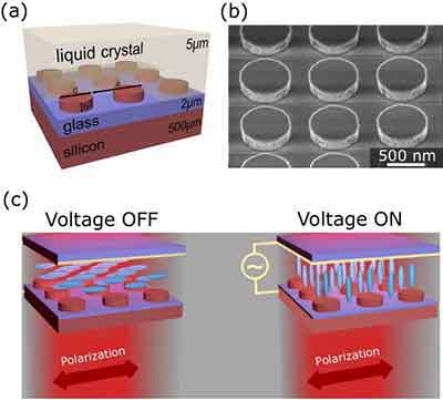
Compare Common Glass Wafer Materials
The best glass wafer material depends on the thermal, optical, electrical, and mechanical requirements of the application. The table below compares several commonly requested substrate families.
| Glass Type | Key Properties | Typical Applications | Common Processing |
|---|---|---|---|
| Borosilicate Glass | Low thermal expansion, good chemical resistance, optical transparency, and compatibility with silicon bonding processes. | MEMS, microfluidics, sensors, wafer-level packaging, optical caps, and lab-on-chip devices. | Anodic bonding, polishing, wet etching, laser machining, coating, and thin-film deposition. |
| Fused Silica | Very low thermal expansion, high purity, excellent thermal-shock resistance, and broad optical transmission. | UV optics, photonics, spectroscopy, lithography, laser systems, and high-temperature research. | Optical polishing, fluorine-based etching, laser machining, coatings, and precision fabrication. |
| D263 Thin Glass | Thin, smooth glass with good optical quality, dimensional uniformity, and availability in precision thicknesses. | Displays, micro-optics, sensors, thin-film devices, microfluidics, and research substrates. | Cutting, polishing, coating, thin-film deposition, lithography, and bonding. |
| BK7 Optical Glass | Good visible-light transmission, optical uniformity, and established use in optical systems. | Optical experiments, imaging, lenses, windows, photonics, and spectroscopy. | Optical polishing, coating, cutting, drilling, and precision machining. |
| Soda-Lime Glass | Economical, readily available, transparent, and suitable for less demanding research and testing applications. | Test substrates, optical windows, educational research, displays, and prototype devices. | Cutting, polishing, coating, drilling, and basic microfabrication. |
Borosilicate Glass Wafers
Borosilicate glass wafers are widely used in MEMS, microfluidics, sensors, and wafer-level packaging because they combine good chemical durability with relatively low thermal expansion. Certain sodium-containing borosilicate glasses are particularly useful for anodic bonding to silicon.
UniversityWafer supplies materials such as Borofloat® 33 and other borosilicate substrates for research, prototyping, bonding, micromachining, and device fabrication.
Fused Silica and Quartz Wafers
Fused silica wafers are commonly selected when high optical transmission, low thermal expansion, low impurity levels, or resistance to thermal shock is important. These properties make fused silica useful for photonics, UV processing, spectroscopy, laser systems, semiconductor research, and optical devices.
Fused silica can also be polished to very smooth surfaces and processed using laser machining, lithography, thin-film deposition, and fluorine-based etching techniques.
D263, BK7, Corning and Specialty Glass
UniversityWafer also supplies specialty glass substrates for applications that require specific thicknesses, optical properties, surface finishes, or device compatibility.
- D263 Glass – Thin glass commonly used in displays, micro-optics, sensors, microfluidics, and thin-film research.
- BK7 Glass – Optical glass used for imaging, photonics, spectroscopy, and precision optical applications.
- Corning Glass – Specialty display and electronics glass for thin-film, optical, and electronic device research.
- Soda-Lime Glass – Cost-effective glass for testing, windows, displays, and prototype applications.
Glass Wafer Sizes and Specifications
Glass wafer specifications can be selected to match lithography, bonding, optical, microfluidic, and semiconductor fabrication requirements. Availability depends on the glass composition and requested geometry.
- Diameter: Common diameters include 50 mm, 100 mm, 150 mm, 200 mm, and 300 mm, with custom dimensions available for many materials.
- Thickness: Standard, thin, ultra-thin, and custom thickness substrates are available depending on material and application.
- Surface Finish: Single-side polished (SSP), double-side polished (DSP), and optical-grade polished surfaces can be specified.
- Flatness and TTV: Low bow, warp, and total thickness variation (TTV) can be important for wafer bonding, lithography, and precision assembly.
- Surface Roughness: High-quality polished glass can be supplied for optical, thin-film, bonding, and microfabrication applications.
- Edges and Geometry: Round wafers, custom shapes, flats, notches, chamfered edges, and other geometries may be available.
Glass Wafer Coatings and Thin Films
Glass substrates can be supplied or processed with coatings and thin films that add optical, electrical, or surface functionality.
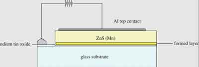
- ITO coatings for transparent conductive electrodes.
- Metal films such as chromium and gold for electrodes, adhesion layers, and device fabrication.
- Anti-reflective and optical coatings for photonics, imaging, and display research.
- Hydrophilic or hydrophobic surface treatments for microfluidic and biosensing applications.
- Dielectric layers for optical, electronic, and thin-film device development.
Glass Wafer Micromachining and Processing
Glass wafers can be processed using several techniques depending on material composition, thickness, feature size, and final application.
- Laser Cutting and Drilling: Used to produce holes, channels, slots, cavities, and custom wafer geometries.
- Wet Etching: HF-based chemistries may be used to etch silica-based glass materials and form channels or cavities.
- Dry Etching: Plasma processes can be used for selected fused silica, quartz, and glass microfabrication applications.
- Polishing and Lapping: Used to control thickness, flatness, surface finish, and optical quality.
- Through-Glass Features: Holes and through-glass vias can be used for advanced packaging, sensors, MEMS, and electrical interconnects.
Glass-to-Silicon and Glass-to-Glass Bonding
Glass wafers are frequently bonded to silicon or other glass substrates during MEMS, microfluidic, sensor, optical, and packaging fabrication. The correct glass composition should be selected based on temperature, surface quality, CTE compatibility, and the intended bonding method.
Anodic Bonding
Anodic bonding is commonly used to join silicon to compatible alkali-containing glass. It is widely used for MEMS caps, pressure sensors, microfluidic structures, and hermetic or semi-hermetic device packaging.
Glass-to-Glass Bonding
Glass wafers can also be joined using fusion bonding, adhesive bonding, intermediate layers, and other methods depending on the thermal budget and device requirements.
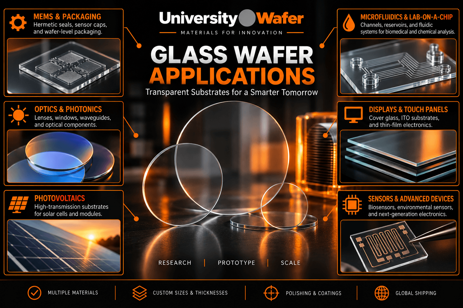
Applications for Glass Wafers
Glass wafers are used across research, development, prototyping, and specialized manufacturing applications.
- MEMS devices and wafer-level packaging
- Microfluidic channels and lab-on-chip devices
- Pressure sensors and optical sensors
- Photonics and optical research
- UV lithography and spectroscopy
- Displays and transparent electronics
- ITO electrodes and thin-film devices
- Biosensors and diagnostic devices
- Through-glass vias and advanced packaging
- Silicon-to-glass bonding
- Solar and photovoltaic research
How to Select a Glass Wafer
Before requesting a quote, identify the parameters that are most important to your process. Providing these specifications helps determine which glass substrate is best suited for your experiment or device.
- Glass material or composition
- Diameter or custom dimensions
- Wafer thickness
- Thickness tolerance
- Single-side or double-side polish
- Surface roughness
- Bow, warp, and TTV requirements
- Optical transmission range
- Coating or thin-film requirements
- Bonding process
- Etching or micromachining requirements
- Quantity
Why Researchers Choose UniversityWafer
- Single-wafer and small-quantity orders for research, development, and prototyping.
- Multiple glass materials and substrate formats.
- Custom thicknesses, diameters, polish options, coatings, and processing services.
- Technical support for selecting glass wafers based on optical, thermal, bonding, and fabrication requirements.
- Fast quote turnaround and worldwide shipping.
Related Glass Wafer Resources
- Glass Substrates – Learn about glass substrate materials, properties, and research applications.
- Borofloat® 33 Glass Wafers – Borosilicate glass for MEMS, microfluidics, sensors, and silicon-to-glass bonding.
- Borosilicate Glass Wafers – Explore borosilicate substrates for microfabrication, optics, bonding, and research.
- Fused Silica Wafers – High-purity substrates for UV optics, photonics, spectroscopy, and thermal applications.
- Quartz Substrates – Quartz materials for optical, photonic, semiconductor, and research applications.
- D263 Glass Wafers – Thin specialty glass for displays, sensors, micro-optics, and thin-film devices.
- BK7 Optical Glass – Optical glass substrates for imaging, photonics, spectroscopy, and laboratory research.
- Corning Eagle Glass – Specialty glass for display, electronics, optical, and thin-film research.
- Ultra-Thin Glass – Thin glass substrates for compact devices, displays, sensors, and advanced research.
- ITO-Coated Glass Wafers – Transparent conductive substrates for displays, sensors, photovoltaics, and thin-film devices.
- Microfluidic Substrates – Substrate options for channels, lab-on-chip devices, biosensors, and fluidic research.
- MEMS Substrates – Materials for MEMS sensors, packaging, micromachining, and wafer-level devices.
- Silicon-on-Glass (SOG) – Learn about silicon and glass integration for MEMS, sensors, and advanced devices.
- Total Thickness Variation (TTV) – Understand wafer thickness uniformity for bonding, lithography, and precision processing.