
Buy Silicon Wafers for Research & Manufacturing
UniversityWafer supplies high-quality silicon wafers for semiconductor fabrication, MEMS, photolithography, thin film deposition, sensors, optics, and university research. Standard inventory is available for fast delivery, and custom wafer specifications can be manufactured upon request.
Get Your Silicon Wafer Quote FAST! Or, Buy Online and Start Researching Today!
Custom Specifications Available
Need a custom wafer? We offer a wide variety of diameters, crystal orientations, dopants, resistivities, thicknesses, polish options, oxide layers, and other specifications for research and production applications. Contact our team today for a fast quotation.
How to Buy Silicon Wafers
Whether you're developing semiconductor devices, MEMS sensors, photonic components, or university research projects, selecting the right silicon wafer is critical to achieving consistent results. UniversityWafer supplies research-grade silicon substrates in a wide range of diameters, orientations, dopants, resistivities, and surface finishes to meet the needs of researchers and manufacturers worldwide.
What Should You Consider Before Buying Silicon Wafers?
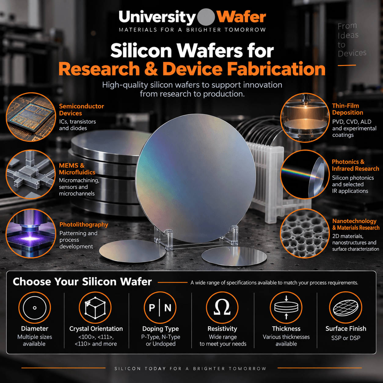
Before placing an order, it is helpful to determine the specifications required for your process. Important wafer characteristics include:
- Diameter: Available from small diced substrates up to 300 mm wafers.
- Crystal Orientation: (100), (111), (110), (211), and custom orientations.
- Dopant Type: Boron (P-type), Phosphorus, Arsenic, or Antimony (N-type), or intrinsic silicon.
- Resistivity: Low, standard, or high-resistivity silicon for RF and detector applications.
- Thickness: Standard or custom thicknesses depending on your fabrication process.
- Surface Finish: SSP, DSP, etched, lapped, or epi-ready.
Common Applications
Silicon wafers serve as the foundation for countless electronic and scientific applications, including:
- Semiconductor device fabrication
- Photolithography
- MEMS fabrication
- Thin film deposition
- Solar cell development
- Power electronics
- SOI device fabrication
- Thermal oxide processing
Prime, Test, and Research Wafers
Depending on your project, you may choose from prime-grade production wafers, economical test wafers, reclaimed wafers, or custom research substrates. UniversityWafer also supplies oxidized wafers, nitride-coated wafers, SOI wafers, and epitaxial silicon wafers for specialized applications.
Why Researchers Choose UniversityWafer
Our customers include universities, government laboratories, startups, and Fortune 500 semiconductor companies. Whether you need a single prototype wafer or high-volume production quantities, our experienced team can help you select the right substrate for your application and provide fast quotations on standard or custom specifications.