
Choosing the Correct Silicon Wafer Orientation
Silicon wafer orientation describes the crystallographic plane parallel to the wafer surface. The most common orientations are (100), (110), and (111), written using Miller indices. Because single-crystal silicon is anisotropic, its mechanical, electrical, oxidation, and etching behavior can depend on crystallographic direction.
Choosing the correct orientation is therefore important for semiconductor fabrication, MEMS, anisotropic wet etching, wafer bonding, sensors, microfluidics, and crystallographic research.
UniversityWafer supplies silicon wafers in standard and specialty orientations, including (100), (110), (111), and selected off-axis or research cuts.
Need a Specific Silicon Crystal Orientation?
UniversityWafer supplies silicon substrates in common and specialty crystallographic orientations for semiconductor fabrication, MEMS, anisotropic etching, surface science, epitaxy, sensors, and research.
Get Your Silicon Wafer Orientation Quote FAST! Or, Buy Wafers Online and Start Researching Today!
What Do (100), (110), and (111) Mean?
The numbers in parentheses are Miller indices, a notation used to identify crystallographic planes in a crystal lattice. For a silicon wafer, the stated orientation identifies the crystal plane that is nominally parallel to the polished wafer surface.
- (100) silicon: One of the most widely used orientations for semiconductor and MOS device fabrication.
- (110) silicon: Important in selected MEMS, anisotropic-etching, and device-research applications.
- (111) silicon: The most densely packed low-index surface of diamond-cubic silicon and important in crystallographic, epitaxial, and anisotropic-etching research.
(100) Silicon Wafers
(100) silicon wafers are widely used in integrated-circuit and MOS fabrication. The Si/SiO2 interface on properly processed (100) silicon has historically been favorable for MOS technology, which helped make (100) the dominant orientation for many silicon IC processes.
(100) wafers are also widely used in MEMS and micromachining. When anisotropically etched with solutions such as KOH or TMAH, the slowly etched {111} planes can form characteristic sloped sidewalls. On a (100) wafer, these {111} planes intersect the wafer surface at approximately 54.7°.
This geometry is useful for forming V-grooves, pyramidal cavities, diaphragms, and other crystallographically defined structures.
(110) Silicon Wafers
(110) silicon wafers are particularly useful in some MEMS and anisotropic wet-etching applications.
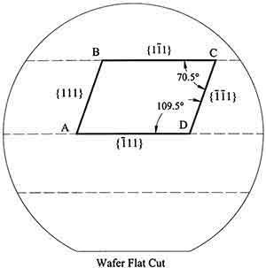
For appropriately aligned patterns on a (110) wafer, selected {111} planes can be perpendicular to the wafer surface. Because {111} planes etch much more slowly than many other silicon planes in alkaline anisotropic etchants, this geometry can be exploited to form nearly vertical crystallographic sidewalls.
Exact sidewall geometry depends on mask alignment, etchant chemistry, temperature, concentration, doping, and feature orientation, so (110) silicon should not be treated as automatically producing vertical walls for every mask layout.
(111) Silicon Wafers
(111) silicon wafers expose the most densely packed low-index surface of crystalline silicon. The {111} family of planes is especially important in anisotropic wet etching because these planes generally etch more slowly than many other crystallographic planes in commonly used alkaline silicon etchants.
(111) silicon is used in selected semiconductor, epitaxial, surface-science, detector, sensor, and micromachining applications where crystallographic orientation is important.
It is better to choose (111) based on the specific process requirements rather than assuming it is inherently a "power-device orientation." Modern power-device architectures use several substrate orientations depending on device type and fabrication technology.
Silicon Orientation and Anisotropic Wet Etching
One of the most important reasons to specify crystal orientation is anisotropic silicon etching. In alkaline etchants such as potassium hydroxide (KOH) or tetramethylammonium hydroxide (TMAH), different crystallographic planes can etch at very different rates.
The relatively slow etch rate of {111} planes allows wafer orientation and mask alignment to determine the final shape of etched structures. This property is widely exploited in MEMS, microfluidics, sensors, V-grooves, cavities, membranes, and other micromachined structures.
Learn more about silicon wafers for anisotropic etching .
Silicon Orientation and CMOS Fabrication
(100) silicon became widely used in MOS and CMOS technology in part because of favorable electrical characteristics at the properly prepared Si/SiO2 interface. Interface quality is influenced by crystal orientation as well as oxidation conditions, cleaning, contamination, dielectric processing, and subsequent device fabrication.
Orientation also affects direction-dependent carrier transport and mechanical properties. In advanced transistor research, engineers can exploit specific crystal directions and channel orientations to optimize electron or hole transport.
Surface Orientation vs. Crystal Direction
It is important to distinguish between a crystallographic plane and a crystallographic direction. Planes are normally written with parentheses, such as (100), while directions are written with square brackets, such as [100].
Families of equivalent planes may be written with braces, such as {111}, while families of equivalent directions may be written with angle brackets, such as <110>.
For wafer specifications, it is usually clearer to describe the surface orientation as (100), (110), or (111) rather than using angle brackets.
Wafer Flats, Notches, and Crystal Orientation
Wafer flats and notches provide physical reference features used for wafer alignment, handling, and identification. They are not thermal barriers and do not prevent heat from entering the wafer.
Older and smaller-diameter wafers commonly use one or more flats, while modern larger wafers typically use a notch to preserve more usable wafer area. Samsung notes that notched wafers allow more dies to be produced than wafers using a large flat because less edge area is removed.
The relationship between a flat or notch and crystallographic direction depends on the applicable wafer specification, so researchers should confirm the orientation from the wafer certificate of analysis (COA) or supplier documentation rather than relying only on appearance.
See the Silicon Wafer Flats Guide for additional information.
Can You Determine Orientation by Breaking a Silicon Wafer?
Silicon cleaves preferentially along crystallographic planes, so fracture patterns can sometimes provide qualitative information about wafer orientation. However, deliberately breaking or striking a wafer is destructive and not a reliable metrology method.
Fracture behavior depends on wafer orientation, edge condition, pre-existing defects, surface damage, applied stress, and the direction in which the force is introduced.
For reliable orientation verification, use documented supplier specifications or crystallographic measurement techniques such as X-ray diffraction (XRD).
How Is Silicon Wafer Orientation Verified?
X-ray diffraction can be used to determine the orientation of crystalline silicon by measuring diffraction from specific lattice planes. During wafer manufacturing, crystallographic measurements help align the silicon crystal before slicing and can verify wafer orientation or intentional off-axis miscut.
The achievable measurement uncertainty depends on the instrument, measurement geometry, alignment method, and calibration, so one universal accuracy value should not be assumed for every XRD system.
Which Silicon Wafer Orientation Should I Choose?
The correct orientation depends on the fabrication process rather than one orientation being universally "best."
- CMOS / MOS research: (100) is widely used for conventional silicon device fabrication.
- KOH or TMAH etching: Select orientation and mask alignment according to the required crystallographic sidewall geometry.
- MEMS with vertical crystallographic walls: (110) can be advantageous for appropriately aligned anisotropic etch structures.
- V-grooves and pyramidal structures: (100) is commonly used to expose slow-etching {111} sidewalls.
- Surface-science or epitaxial research: (111), (100), or other orientations may be selected according to the desired surface symmetry and growth behavior.
- Custom crystallographic research: off-axis or higher-index orientations may be required.
Available Silicon Wafer Orientations
- (100) Silicon Wafers – widely used in MOS, CMOS, IC, MEMS, and anisotropic etching.
- (111) Silicon Wafers – useful for crystallographic, surface, epitaxial, and etching research.
- (110) Silicon Wafers – useful for selected MEMS and anisotropic-etch geometries.
- Specialty Silicon Orientations – including selected higher-index and research cuts.
How to Specify Silicon Wafer Orientation
When requesting a silicon wafer quote, include both the crystallographic orientation and the other wafer parameters required by your process. Useful specifications include:
- Surface orientation – (100), (110), (111), or custom
- Orientation tolerance or miscut
- Diameter
- Thickness
- Growth method – CZ or FZ
- Conductivity type – P-type or N-type
- Dopant
- Resistivity
- SSP or DSP surface finish
- Flat or notch requirements
- Quantity
What Is Silicon Wafer Orientation?
Silicon wafer orientation identifies the crystallographic plane that is nominally parallel to the wafer surface. Because silicon is a single-crystal material with a diamond-cubic crystal structure, many of its physical and processing properties depend on crystallographic direction.
Common silicon wafer surface orientations include (100), (110), and (111). These planes are described using Miller indices, a standard crystallographic notation.
Orientation can influence anisotropic etching, surface atomic arrangement, oxidation behavior, carrier transport along particular directions, mechanical response, cleavage, epitaxial growth, and other fabrication processes. The importance of each effect depends on the specific device and process.
What Are Miller Indices?
Miller indices are a mathematical notation used to describe planes and directions in crystalline materials.
The notation is important because parentheses, brackets, braces, and angle brackets have different meanings:
- (100) – one specific crystallographic plane
- {100} – the family of symmetry-equivalent {100} planes
- [100] – one specific crystallographic direction
- <100> – the family of symmetry-equivalent <100> directions
Therefore, when describing the surface of a silicon wafer, expressions such as (100), (110), and (111) are generally the most appropriate notation.
Why Does Silicon Crystal Orientation Matter?
Silicon is anisotropic, meaning some material properties vary with crystallographic direction. This is particularly important in processes that interact directly with the crystal lattice.
Orientation can be important for:
- Anisotropic wet etching
- MEMS micromachining
- MOS and CMOS processing
- Surface and interface research
- Mechanical and fracture studies
- Epitaxial growth
- Wafer bonding
- Sensor fabrication
- Microfluidic structures
- Crystallographic research
Orientation is only one wafer specification. Dopant, resistivity, crystal-growth method, thickness, surface finish, defects, and film structure can be equally important depending on the application.
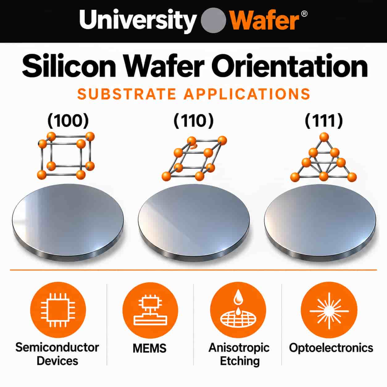
(100) Silicon Wafer Orientation
(100) silicon is one of the most widely used orientations in semiconductor manufacturing. It has been particularly important for MOS and CMOS technology.
One reason for its widespread use is the favorable electrical quality that can be achieved at a properly processed Si/SiO2 interface on (100) silicon. This helped establish (100) as a standard substrate orientation for many silicon integrated-circuit processes.
(100) silicon is also important in MEMS and anisotropic wet etching. In alkaline etchants such as KOH or TMAH, slow-etching {111} planes can become exposed and form sidewalls inclined approximately 54.7° relative to a (100) surface.
This crystallographic geometry can be used to fabricate V-grooves, pyramidal cavities, membranes, channels, and other micromachined structures.
(110) Silicon Wafer Orientation
(110) silicon wafers are used in selected MEMS, semiconductor, and crystallographic research applications.
An important feature of the (110) surface is that certain {111} planes are perpendicular to it. Because {111} planes are comparatively slow-etching in common alkaline anisotropic silicon etchants, properly oriented mask patterns on (110) wafers can be used to produce nearly vertical crystallographically defined sidewalls.
This result depends on mask alignment and process conditions. Simply using a (110) wafer does not guarantee vertical walls for every feature orientation or etch process.
(111) Silicon Wafer Orientation
(111) silicon exposes the most densely packed low-index surface of diamond-cubic silicon.
The {111} family of planes is especially important in anisotropic micromachining because these planes generally etch much more slowly than several other silicon planes in alkaline etchants such as KOH and TMAH.
(111) substrates are also used in selected surface-science, epitaxial-growth, sensor, detector, and semiconductor research applications where surface symmetry or crystallographic orientation is important.
Orientation should be selected according to the actual device and fabrication process rather than assuming (111) is inherently a "power-device orientation."
(100) vs. (110) vs. (111) Silicon Wafers
| Orientation | Important Characteristics | Common Research Uses |
|---|---|---|
| (100) | Widely used semiconductor surface; favorable Si/SiO2 interface characteristics; {111} sidewalls form approximately 54.7° angles during idealized anisotropic etching. | MOS/CMOS research, IC fabrication, MEMS, V-grooves, cavities and anisotropic etching. |
| (110) | Selected {111} planes are perpendicular to the (110) surface, enabling vertical crystallographic sidewalls with appropriately aligned anisotropic etch masks. | MEMS, deep wet-etched structures, sensors and crystallographic research. |
| (111) | Most densely packed low-index silicon surface; {111} planes are comparatively resistant to many alkaline anisotropic etchants. | Surface science, epitaxy, anisotropic-etch studies, sensors and specialized semiconductor research. |
How Does Crystal Orientation Affect KOH Etching?
Potassium hydroxide (KOH) is commonly used for anisotropic wet etching of crystalline silicon. The etch rate depends strongly on crystallographic orientation.
Under typical KOH etching conditions, {111} planes etch substantially more slowly than several other low-index planes. As faster-etching material is removed, slow-etching {111} surfaces can become the boundaries of the resulting structure.
This behavior allows engineers to use the starting wafer orientation and mask alignment to control the geometry of etched structures.
Actual etch rates and selectivity depend on variables including:
- KOH concentration
- Temperature
- Crystal orientation
- Doping concentration
- Mask orientation
- Agitation and process conditions
- Surface condition
Therefore, crystallographic geometry should be considered together with the specific etch recipe.
Why Does (100) Silicon Form 54.7° Sidewalls?
During anisotropic etching of a (100) silicon wafer, slowly etched {111} planes can become exposed and bound the etched cavity.
The crystallographic angle between the (100) and (111) planes is approximately 54.74°. This produces the familiar sloped sidewalls seen in KOH- or TMAH-etched (100) silicon structures.
This geometry is widely exploited for silicon V-grooves, pyramidal pits, cavities, membranes, microfluidic features, and MEMS structures.
Does Silicon Orientation Affect Oxidation?
Yes. Thermal oxidation kinetics can depend on silicon surface orientation, particularly during portions of the oxidation process where the Si/SiO2 interface reaction contributes significantly to the overall growth rate.
However, oxidation rate is also strongly affected by temperature, dry versus wet oxidation, pressure, dopant concentration, oxide thickness, and process history.
It is therefore more accurate to treat crystal orientation as one variable affecting oxidation behavior rather than saying one orientation is universally "easier to oxidize."
Does Silicon Orientation Affect Ion Implantation?
Crystal orientation can influence ion channeling during ion implantation. If incoming ions are closely aligned with major crystallographic directions or planes, some ions can travel farther through relatively open channels in the crystal lattice than predicted for an amorphous target.
Semiconductor implantation processes commonly use controlled wafer tilt and rotation to reduce unwanted channeling. Implant depth is not determined by orientation alone; it also depends on ion species, implantation energy, dose, wafer temperature, surface films, tilt, rotation, and subsequent thermal processing.
Does Silicon Orientation Affect Carrier Mobility?
Charge-carrier transport in silicon is also anisotropic. Electron and hole transport can depend on the orientation of the wafer surface and the direction of current flow relative to the crystal lattice.
This is particularly important in advanced transistor research, where device orientation, channel direction, strain, confinement, and surface orientation can be engineered to optimize electrical performance.
Consequently, there is no single wafer orientation that provides the highest mobility for every carrier type and device architecture.
Wafer Flats, Notches and Crystal Orientation
A wafer flat or notch is a physical reference feature used for wafer alignment, handling, and—in some wafer standards—identification of crystallographic or conductivity information.
Flats and notches do not control heat conduction through the wafer. They are geometric reference features.
Smaller and legacy silicon wafers commonly use flats, while larger semiconductor wafers commonly use a notch. The exact relationship between the reference feature and crystal direction should be interpreted according to the applicable wafer specification.
Learn more in the Silicon Wafer Flats & Notches Guide.
Can Breaking a Wafer Determine Its Orientation?
Silicon is a brittle single crystal and can exhibit preferred fracture behavior related to its crystallography. Demonstrations involving scribing or breaking wafers can therefore show different fracture patterns for different orientations.
However, a destructive fracture test should not be treated as a precise or definitive method of identifying an unknown wafer. Fracture behavior also depends on edge defects, scratches, wafer thickness, applied stress, scribe direction, and other mechanical conditions.
If orientation is important to a fabrication process, use supplier documentation, wafer identification specifications, or a crystallographic measurement technique such as X-ray diffraction.
Video: Silicon Wafer Cleavage and Orientation
How Is Silicon Wafer Orientation Measured?
X-ray diffraction (XRD) is a standard technique for determining crystallographic orientation. X-rays incident on a single crystal produce diffraction according to the spacing and orientation of atomic lattice planes.
During silicon crystal and wafer manufacturing, X-ray-based crystallographic measurements can be used to orient the crystal before slicing and to verify the resulting wafer surface orientation or intentional miscut.
The measurement uncertainty depends on the diffraction instrument, alignment procedure, measurement geometry, calibration, and required specification. A universal accuracy value should therefore not be assigned to all XRD orientation measurements.
What Is an Off-Axis or Miscut Silicon Wafer?
A silicon wafer does not always need to be cut exactly parallel to a low-index crystal plane. An off-axis or miscut wafer is intentionally cut at a specified small angle away from a nominal orientation such as (100) or (111).
Miscut angle and direction can influence surface step structure and can be important in selected epitaxial-growth, surface-science, and device-research applications.
When ordering an off-axis wafer, specify both the miscut angle and miscut direction, along with the nominal surface orientation.
Crystal Orientation vs. Wafer Growth Method
Silicon crystal orientation and silicon crystal-growth method are different specifications.
Czochralski (CZ) silicon is grown from molten silicon using a seed crystal that establishes the crystallographic orientation of the growing ingot.
Float-zone (FZ) silicon is produced by moving a molten zone through a silicon rod while maintaining single-crystal growth. FZ material is often selected when very high resistivity or relatively low oxygen concentration is required.
Both CZ and FZ silicon can be produced in specified crystallographic orientations. Therefore, growth method and wafer orientation should be specified independently.
Standard vs. Custom Silicon Crystal Orientations
Most semiconductor research uses common low-index orientations such as (100), (110), or (111), but specialty applications can require higher-index surfaces or intentionally miscut substrates.
UniversityWafer can supply standard and specialty silicon orientations for research involving semiconductor processing, epitaxy, MEMS, crystallography, anisotropic etching, sensors, and surface science.
When requesting a specialty orientation, provide the nominal plane, orientation tolerance, miscut angle and direction when applicable, wafer diameter, thickness, dopant, resistivity, growth method, and surface-polish requirements.
Silicon Wafer Orientation FAQ
What is the most common silicon wafer orientation?
(100) is one of the most widely used silicon wafer orientations, particularly for MOS/CMOS and general semiconductor fabrication.
Which silicon orientation is commonly used for KOH etching?
Both (100) and (110) silicon can be useful for anisotropic KOH etching, depending on the desired geometry. (100) wafers are commonly used to form structures bounded by inclined {111} surfaces, while properly aligned patterns on (110) wafers can expose {111} planes approximately perpendicular to the wafer surface.
Why are (111) planes important in silicon etching?
{111} planes generally etch relatively slowly in common alkaline anisotropic silicon etchants. As faster-etching planes are removed, {111} surfaces can become the crystallographically defined boundaries of the etched structure.
What is the difference between (100) and <100>?
(100) describes a specific crystallographic plane, while <100> describes the family of symmetry-equivalent crystallographic directions.
How can I verify an unknown silicon wafer orientation?
Check the wafer certificate or supplier documentation first. When independent crystallographic verification is required, X-ray diffraction can be used to determine crystal orientation.