
Dielectric Oxide Wafers and Thin Films for Research
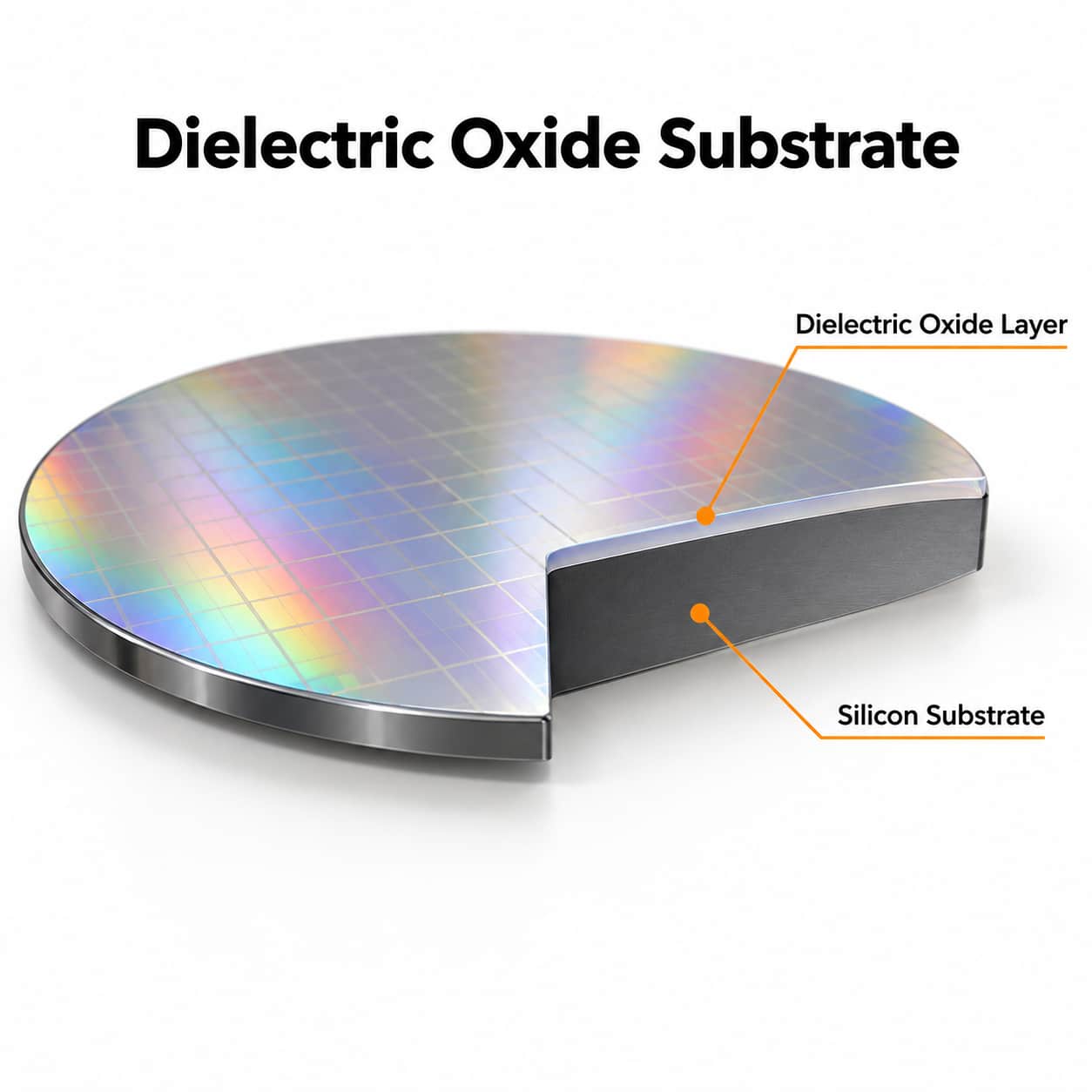
UniversityWafer supplies substrates for research involving dielectric oxides, gate insulators, semiconductor passivation, capacitors, MEMS, sensors, and optical thin films. Researchers can select from silicon wafers, oxidized silicon substrates, specialty semiconductor wafers, and other materials suitable for dielectric thin-film deposition.
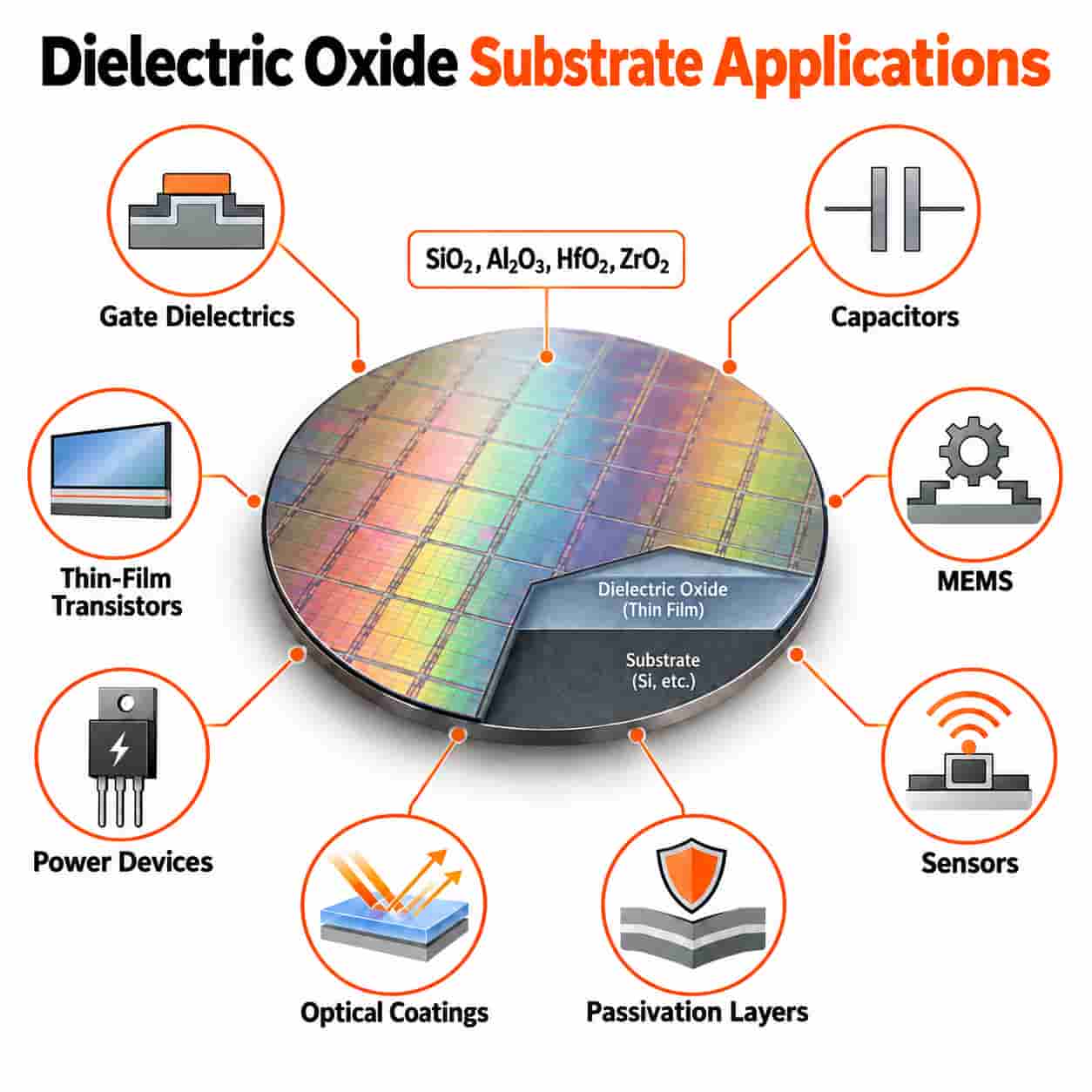
Common dielectric materials used in electronic and photonic research include SiO2, Al2O3, HfO2, ZrO2, and Ta2O5. Material selection depends on the required dielectric constant, electrical insulation, interface quality, optical properties, film thickness, and processing conditions.
Silicon Wafers with Dielectric Layers
Silicon is one of the most common substrates for dielectric oxide research. UniversityWafer supplies silicon wafers in a variety of diameters, orientations, thicknesses, resistivities, and surface finishes for thin-film deposition and semiconductor fabrication.
Researchers requiring a pre-grown SiO2 layer can use thermal oxide silicon wafers. Thermal oxidation produces SiO2 directly from the silicon surface and is widely used for electrical insulation, MOS structures, MEMS, surface passivation, and device fabrication.
Dielectric Oxides for Gate Insulation
A gate dielectric electrically separates a transistor gate electrode from the semiconductor channel while allowing the gate electric field to control carrier concentration in the device.
Traditional devices frequently use SiO2, while advanced structures may use high-k dielectric oxides such as HfO2 or Al2O3. High-k materials can provide greater capacitance at a larger physical thickness than SiO2, which can help reduce direct tunneling leakage.
Learn more about gate dielectric materials used in MOS devices and transistor research.
Common Dielectric Oxide Applications
- MOS and MOSFET gate dielectrics
- Capacitors and energy-storage structures
- Electrical isolation layers
- Semiconductor surface passivation
- MEMS and microfabricated devices
- Thin-film transistors
- Power semiconductor devices
- Sensors and detector structures
- Optical interference coatings
- Photonic and optoelectronic devices
Dielectric Films for Advanced Semiconductors
Dielectric layers are also important in devices fabricated on silicon carbide (SiC) and gallium nitride (GaN). These wide-bandgap semiconductors are widely researched for high-power, high-voltage, and high-frequency electronics.
In these systems, dielectric films can serve as gate insulators, passivation layers, or electrical isolation layers. The quality of the dielectric-semiconductor interface can strongly affect device performance and reliability.
Specify Your Dielectric Oxide Research Requirements
When requesting substrates for dielectric oxide research, please include as much information as possible about your application. Useful specifications may include:
- Substrate material
- Wafer diameter or dimensions
- Crystal orientation
- Wafer thickness
- Resistivity or conductivity type
- Desired dielectric material
- Dielectric film thickness
- Single-side or double-side polish
- Surface roughness requirements
- Quantity
Get Your Dielectric Oxide Substrate Quote FAST! Or, Buy Research Substrates Online and start researching today.
What Are Dielectric Oxides?
Dielectric oxides are electrically insulating oxide materials that can store electrical energy when exposed to an electric field. In semiconductor devices, dielectric layers are commonly used to electrically isolate conductive regions, control capacitance, protect surfaces, and form gate insulating layers.
Important dielectric oxide materials include silicon dioxide (SiO2), aluminum oxide (Al2O3), hafnium oxide (HfO2), zirconium oxide (ZrO2), and tantalum pentoxide (Ta2O5). The appropriate material depends on the required dielectric constant, film thickness, breakdown strength, interface quality, optical properties, and fabrication process.
Dielectric Oxides in Semiconductor Devices
Dielectric oxide layers are essential in many semiconductor structures. In a MOS device, for example, a dielectric separates the gate electrode from the semiconductor while allowing the electric field from the gate to control charge in the underlying channel.
Researchers developing MOSFETs, thin-film transistors, sensors, MEMS, and other electronic devices often require carefully controlled gate dielectric materials. Important properties include low leakage current, high electrical breakdown strength, low defect density, suitable dielectric constant, and a stable interface with the semiconductor.
Silicon Dioxide (SiO2)
Silicon dioxide is one of the most widely studied dielectric materials in semiconductor technology. SiO2 has a relative dielectric constant of approximately 3.9 and can form a high-quality interface directly with silicon.
Silicon wafers can be thermally oxidized to create precisely controlled insulating layers for MOS structures, microelectronics, MEMS fabrication, research devices, and surface passivation. UniversityWafer supplies thermal oxide silicon wafers with different oxide thicknesses and wafer specifications.
High-k Dielectric Oxides
As semiconductor devices became smaller, extremely thin SiO2 layers became increasingly susceptible to electron tunneling and leakage. This led to the development of high-k dielectric materials, which have a higher dielectric constant than SiO2.
Materials such as hafnium oxide (HfO2) and aluminum oxide (Al2O3) can provide greater capacitance for a given physical thickness than SiO2. A physically thicker high-k dielectric can therefore provide the required electrical capacitance while helping reduce direct tunneling current.
HfO2, in particular, became an important high-k gate dielectric for advanced CMOS technology because of its relatively high dielectric constant, suitable bandgap, and compatibility with semiconductor processing.
Aluminum Oxide (Al2O3) Dielectrics
Aluminum oxide is another important dielectric material. Al2O3 has a higher dielectric constant than SiO2, strong electrical insulation, a wide bandgap, and good chemical and thermal stability.
Aluminum oxide films are studied for semiconductor passivation, transistor gate stacks, sensors, optical coatings, and devices based on wide-bandgap semiconductors. Bulk sapphire (Al2O3) substrates are also widely used in electronic and optical research, although a sapphire wafer and a deposited amorphous Al2O3 dielectric film have different structures and applications.
Dielectric Constant and Capacitance
The dielectric constant, commonly represented by k, describes a material's ability to become electrically polarized and store energy in an electric field. For a simple parallel-plate capacitor, capacitance increases with dielectric constant and decreases as dielectric thickness increases.
This relationship is important in transistor design because a higher-k material can provide a desired gate capacitance using a physically thicker insulating layer. However, dielectric constant alone does not determine whether an oxide is suitable for a device. Researchers must also consider leakage current, band alignment, interface defects, breakdown field, thermal stability, and process compatibility.
Dielectric Oxide Deposition Methods
Dielectric oxide films can be formed using several deposition and growth techniques. The appropriate process depends on the oxide material, required thickness, substrate, temperature limitations, and desired film quality.
- Thermal oxidation: commonly used to grow SiO2 directly on silicon.
- Atomic layer deposition (ALD): widely used for thin, conformal Al2O3, HfO2, and other high-k dielectric films.
- Chemical vapor deposition (CVD/PECVD): used for dielectric and passivation films such as SiO2 and silicon nitride.
- Sputtering: used to deposit a variety of oxide and dielectric thin films. Learn more about sputtered films.
- Electron-beam evaporation: can deposit dielectric materials and multilayer optical structures, including combinations of SiO2 and HfO2. See electron-beam evaporation.
Dielectric Oxides for FET Research
In a field-effect transistor, the gate dielectric must electrically isolate the gate electrode from the semiconductor while still permitting the gate electric field to control the channel. Researchers therefore carefully evaluate dielectric thickness, leakage current, breakdown strength, interface trap density, and surface quality.
Silicon dioxide, aluminum oxide, hafnium oxide, and related dielectric materials are used in field-effect transistor research. The optimum dielectric depends on the semiconductor channel and the electrical requirements of the device.
Dielectrics for SiC and GaN Devices
Advanced power and high-frequency devices frequently use wide-bandgap semiconductor materials such as silicon carbide (SiC) and gallium nitride (GaN). Dielectric layers in these devices may be used for gate insulation, passivation, electrical isolation, or device packaging.
The quality of the dielectric-semiconductor interface is especially important because interface defects and trapped charge can influence threshold voltage, carrier mobility, leakage current, stability, and device reliability.
Dielectric Oxides in MEMS and Sensors
Dielectric films are also important in microelectromechanical systems (MEMS), capacitive sensors, microfabricated structures, and electrically isolated device layers. SiO2 and other insulating materials can provide electrical isolation, structural layers, surface passivation, or sacrificial layers depending on the fabrication process.
Researchers can also use silicon-on-insulator (SOI) wafers when a buried dielectric layer is needed to electrically isolate the device silicon from the handle wafer.
Dielectric Oxides for Optical Coatings
Oxide dielectrics are not limited to electronic devices. Materials such as SiO2, HfO2, TiO2, and Ta2O5 can also be used in optical thin-film stacks. By combining dielectric materials with different refractive indices, researchers can create interference coatings with engineered reflection and transmission properties.
These multilayer structures are used in mirrors, filters, anti-reflection coatings, photonic devices, and related optical coatings.
Choosing a Dielectric Oxide
Selecting a dielectric material requires balancing several electrical, physical, and processing properties. Important specifications may include:
- Dielectric constant (k-value)
- Film thickness and thickness uniformity
- Leakage current
- Electrical breakdown strength
- Bandgap and semiconductor band alignment
- Interface trap density
- Surface roughness
- Thermal and chemical stability
- Deposition or growth temperature
- Compatibility with the underlying substrate
The best dielectric oxide therefore depends on the intended application rather than dielectric constant alone. UniversityWafer can provide silicon wafers, thermal oxide substrates, SOI wafers, and specialty substrates for dielectric thin-film deposition and semiconductor research.