Silicon Dioxide Wafers for Field-Effect Transistor Fabrication
UniversityWafer supplies heavily doped silicon wafers with high-quality
thermal silicon dioxide
for field-effect transistor fabrication, MOSFET research, organic field-effect transistors, back-gated devices, sensors, and semiconductor testing.
Researchers can request custom oxide thicknesses, low-resistivity silicon substrates, dry thermal oxidation, forming-gas annealing, backside metal contacts, and diced samples.
Research Request: Thermal Oxide Wafers for FET Devices
A PhD candidate requested the following wafer specifications:
The researcher also requested information about standard oxide-coated silicon wafers suitable for organic field-effect transistor fabrication.
Reference #267661 for specifications and pricing.
Request a Field-Effect Transistor Wafer Quote
Tell us the substrate material, wafer diameter, orientation, resistivity, oxide thickness, surface finish, backside coating, diced dimensions, and required quantity.
Get Your FET Wafer Quote FAST!
Or,
Buy Online
and start your research today.
What Is a Field-Effect Transistor?
A field-effect transistor, commonly abbreviated as FET, is a voltage-controlled semiconductor device that regulates current through a channel between the source and drain terminals.
Voltage applied to the gate creates an electric field that changes the concentration or movement of charge carriers in the semiconductor channel. This allows the FET to operate as a switch, amplifier, sensor, oscillator, or voltage-control device.
Common Types of FETs
-
MOSFET:
A metal-oxide-semiconductor field-effect transistor that uses an insulating gate dielectric, commonly silicon dioxide.
-
JFET:
A junction field-effect transistor that uses a semiconductor junction to control current through the channel.
-
OFET:
An organic field-effect transistor that uses an organic semiconductor as the active channel material.
-
Graphene FET:
A field-effect transistor that uses graphene as a sensitive conductive channel for electronic or sensing applications.
-
HEMT:
A high-electron-mobility transistor that uses a semiconductor heterojunction to create a high-mobility carrier channel.
FETs are essential components in integrated circuits, computers, smartphones, power electronics, communication systems, displays, biosensors, and many other electronic technologies.
Graphene FET Substrates for Electrical-Charge Detection
Graphene field-effect transistors are frequently studied for biosensors because electrical charges near the graphene surface can change the conductivity of the channel.
A doctoral researcher requested the following substrate specifications:
The research project combines surface-acoustic-wave mass detection with a graphene field-effect transistor designed to detect electrical charge from cancer cells.
-
Substrate:
single-crystal quartz
- Cut: ST-cut, 90°
- Orientation: Y-axis
- Application: Guided Love-wave device with polymer on quartz
- Diameter: 2 inches
- Thickness: Approximately 500 µm
- Quantity: 50–100 substrates
Reference #259037 for specifications and pricing.
Video: Learn About Field-Effect Transistors
Low-Leakage, Pinhole-Free Silicon Dioxide for FET Devices
The electrical quality of the silicon dioxide layer is critical when highly doped silicon is used as a back gate and SiO2 functions as the gate dielectric.
Pinholes, contamination, poor interface quality, or dielectric defects can create excessive leakage current or electrical shorts after a metal contact is deposited on the oxide.
Research Request: High-Quality Si/SiO2 Wafers
A physicist requested:
- Highly doped silicon substrate for use as the gate
-
High-quality, pinhole-free
silicon dioxide
gate dielectric
- Oxide thickness between 200 nm and 500 nm
- Low leakage current after metal deposition
- Reliable dielectric isolation for transistor fabrication
The researcher reported that previously obtained Si/SiO2 wafers produced excessive leakage and, in some cases, direct electrical shorts after metal contacts were evaporated onto the oxide.
Recommended Oxide Process
For transistor applications requiring low leakage and improved dielectric reliability, we recommend
dry chlorinated thermal oxide
followed by a forming-gas anneal.
Dry oxidation generally produces a denser, higher-quality oxide than wet oxidation, while chlorinated oxidation can help reduce mobile-ion contamination. A forming-gas anneal may further improve the silicon-to-oxide interface by reducing electrically active interface defects.
Reference #125269 for specifications and pricing.
Field-Effect Transistor Substrates and Wafer Materials
A field-effect transistor (FET) is a voltage-controlled semiconductor device in which an electric field regulates current through a conductive channel. The principal terminals are the gate, source, and drain. In many devices, a gate dielectric electrically separates the gate electrode from the semiconductor channel.
The substrate, semiconductor channel, gate dielectric, surface quality, doping, and contact materials all influence FET performance. UniversityWafer supplies
silicon wafers,
thermal oxide wafers,
silicon carbide wafers,
gallium arsenide wafers,
and other substrates for FET research and device development.
Three-Inch Silicon Wafers for Organic FET Research
A university assistant professor requested heavily doped silicon wafers for fabricating organic field-effect transistors. In this device structure, the doped silicon substrate functions as the gate while the surface oxide acts as the gate dielectric.
Requested specifications:
- Diameter: 3 inches (76.2 mm)
- Material: Silicon
- Conductivity: P-type
- Dopant: Boron
- Orientation: <100>
- Resistivity: Less than 0.01 ohm-cm
- Thickness: Approximately 380 µm
- Surface finish: Single-side polished
- Application: Organic field-effect transistor fabrication
View available three-inch silicon wafers, including Item #1318.
Reference #99296 for specifications and pricing.
What Is the Field Effect?
In semiconductor devices, the field effect is the change in electrical conductivity produced by an applied electric field. In a FET, voltage applied to the gate changes the concentration or distribution of charge carriers in the channel between the source and drain.
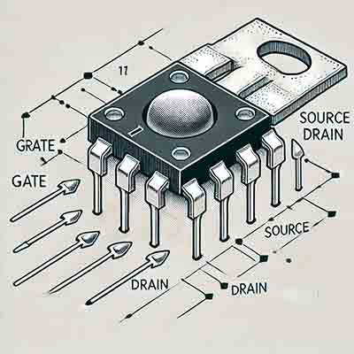 Depending on the device type and gate voltage, the electric field may create, enhance, deplete, or interrupt a conductive channel. This allows the transistor to function as an electronic switch, amplifier, sensor, or signal-control device.
Basic Components of a FET
-
Source:
The terminal through which charge carriers enter the channel.
-
Drain:
The terminal through which charge carriers leave the channel.
-
Gate:
The control electrode that applies the electric field.
-
Channel:
The semiconductor region through which current flows.
-
Gate dielectric:
An insulating layer, such as silicon dioxide or a high-k dielectric, that separates the gate from the semiconductor in insulated-gate devices.
Common Types of Field-Effect Transistors
-
MOSFET:
A metal-oxide-semiconductor field-effect transistor that uses an insulated gate to control current through a semiconductor channel.
-
JFET:
A junction field-effect transistor that uses a reverse-biased semiconductor junction to control channel conductivity.
-
MESFET:
A metal-semiconductor field-effect transistor commonly fabricated with compound semiconductors such as GaAs.
-
HEMT or HFET:
A high-electron-mobility or heterostructure field-effect transistor that uses a heterojunction to form a high-mobility carrier channel.
-
OFET:
An organic field-effect transistor that uses an organic semiconductor as the active channel material.
-
Graphene FET:
A device that uses graphene as a highly sensitive and high-mobility channel material.
-
Thin-Film Transistor:
A FET formed from a deposited semiconductor film, often used in displays, sensors, and flexible electronics.
Gate Dielectrics for FET Fabrication
The gate dielectric is one of the most important layers in an insulated-gate FET. It must electrically isolate the gate while allowing the gate field to control the semiconductor channel.
Thermal silicon dioxide
is widely used because it can form a stable interface with silicon. Researchers may require dry thermal oxide, wet thermal oxide, chlorinated oxide, forming-gas annealing, or custom oxide thicknesses depending on leakage, capacitance, interface-state, and breakdown requirements.
Important Gate-Dielectric Properties
- Oxide or dielectric thickness
- Thickness uniformity
- Low pinhole density
- Low leakage current
- High breakdown strength
- Low interface-trap density
- Low surface roughness
- Controlled dielectric capacitance
Common gate dielectric materials include silicon dioxide, silicon nitride, aluminum oxide, hafnium oxide, and other high-k dielectric films deposited by thermal oxidation, CVD, PECVD, or ALD.
Semiconductor Substrates Used for FET Fabrication
Different semiconductor materials are selected according to the required switching speed, operating voltage, temperature, frequency, optical response, flexibility, or sensing performance.
1. Silicon FET Substrates
Silicon
is the most widely used substrate for MOSFETs, integrated circuits, sensors, MEMS, and power devices. Silicon offers mature fabrication processes, controllable doping, large wafer diameters, and the ability to form a high-quality native silicon dioxide layer.
FET researchers may choose intrinsic, lightly doped, highly doped, or
high-resistivity silicon wafers
depending on whether the substrate serves as the active device layer, back gate, mechanical support, or electrically isolated platform.
2. Germanium FET Substrates
Germanium wafers
offer higher electron and hole mobility than silicon, making germanium attractive for high-speed and low-voltage transistor research.
Germanium device fabrication requires careful control of surface passivation, dielectric interfaces, doping, and contact formation because germanium does not form the same high-quality native oxide interface as silicon.
3. Gallium Arsenide FET Substrates
Gallium arsenide
provides high electron mobility and is widely used for high-frequency, microwave, RF, optoelectronic, MESFET, and HEMT devices.
GaAs does not offer the same native oxide advantages as silicon, so device fabrication often uses Schottky gates, deposited dielectrics, or engineered heterostructures.
4. Indium Phosphide FET Substrates
Indium phosphide
is used in high-speed, millimeter-wave, terahertz, and optical-communication devices. Its high carrier velocity and compatibility with InGaAs and related epitaxial layers make it useful for HEMTs and other heterostructure transistors.
5. Silicon Carbide FET Substrates
Silicon carbide wafers
are used for high-voltage, high-temperature, and high-power field-effect transistors. SiC offers a wide bandgap, high breakdown field, strong thermal conductivity, and good performance in demanding electrical environments.
Common applications include SiC MOSFETs, junction FETs, power converters, electric vehicles, renewable-energy systems, aerospace electronics, and industrial motor drives.
6. Diamond FET Materials
Diamond is one of the most promising semiconductor materials for next-generation
field-effect transistors because of its ultra-wide bandgap, exceptional thermal conductivity,
high carrier mobility, and excellent breakdown electric field. These characteristics make diamond attractive
for experimental high-power, high-frequency, radiation-hardened, and extreme-temperature electronic devices.
Although diamond-based FET technology is still largely confined to research laboratories, continued
improvements in crystal growth, doping techniques, and surface engineering are expanding its potential for
aerospace, defense, nuclear instrumentation, and advanced power electronics.
7. Graphene FET Materials
Graphene
has become one of the most heavily researched materials for field-effect transistor fabrication because of
its exceptional carrier mobility, atomic thickness, mechanical flexibility, and high electrical sensitivity.
Graphene field-effect transistors (GFETs) are widely investigated for biosensors, chemical sensors,
environmental monitoring, RF electronics, wearable devices, and nanoelectronics. Since electrical charges
near the graphene surface directly affect channel conductivity, GFETs are especially useful for label-free
biological sensing.
One challenge is that pristine graphene lacks a natural bandgap, making high on/off switching ratios
difficult for conventional digital logic. Nevertheless, graphene remains one of the leading materials for
sensing and analog electronic applications.
8. Carbon Nanotube Field-Effect Transistors (CNTFETs)
Carbon nanotube field-effect transistors replace the conventional silicon channel with semiconducting
carbon nanotubes. CNTFETs offer extremely small device dimensions, high carrier mobility, and excellent
electrical performance for future low-power integrated circuits.
Current research focuses on improving nanotube alignment, separating metallic from semiconducting nanotubes,
reducing contact resistance, and manufacturing uniform large-area transistor arrays suitable for commercial
semiconductor fabrication.
9. Zinc Oxide FET Materials
Zinc oxide (ZnO)
is a wide-bandgap semiconductor frequently used in thin-film transistors, transparent electronics,
ultraviolet photodetectors, gas sensors, and flexible electronic devices.
ZnO thin films may be deposited onto silicon, sapphire, quartz, glass, or polymer substrates using sputtering,
ALD, CVD, or other thin-film deposition techniques. Device performance depends heavily on crystallinity,
oxygen vacancies, surface morphology, dielectric quality, and interface engineering.
10. Organic Field-Effect Transistors (OFETs)
Organic field-effect transistors utilize organic semiconductor molecules or conductive polymers instead of
crystalline silicon. OFET technology is widely researched for flexible displays, wearable electronics,
printable sensors, RFID tags, electronic skin, and low-cost disposable electronics.
Typical OFET substrate platforms include heavily doped silicon with thermal oxide, glass substrates,
quartz, flexible polymers, and dielectric-coated conductive materials depending on the intended device
architecture.
Graphene FETs for Biosensor Research
Graphene field-effect transistors are particularly valuable for biosensor research because electrical
charges located near the graphene surface directly influence channel conductivity. This enables extremely
sensitive detection of biomolecules, DNA, proteins, viruses, bacteria, ions, gases, and chemical reactions.
A doctoral researcher developing dual biosensors requested
single-crystal quartz substrates
for combining surface-acoustic-wave mass detection with graphene field-effect transistor charge detection.
- Material: Single-crystal quartz
- Cut: ST-cut (90°)
- Orientation: Y-axis
- Diameter: 2 inches
- Thickness: Approximately 500 µm
- Quantity: 50–100 substrates
Reference #259037 for specifications and pricing.
Heterojunction Field-Effect Transistors
A heterojunction field-effect transistor (HFET) combines two or more semiconductor materials
with different band structures to create a high-mobility carrier channel. The interface between these
materials significantly improves carrier transport compared with conventional bulk semiconductor devices.
Common heterostructure systems include AlGaAs/GaAs, AlGaN/GaN, InAlAs/InGaAs, and other III-V compound
semiconductor combinations used in microwave, millimeter-wave, RF, and high-speed communication devices.
AlGaN/GaN High-Electron-Mobility Transistors (HEMTs)
AlGaN/GaN HEMTs
generate a two-dimensional electron gas (2DEG) at the heterojunction without intentional channel doping.
The resulting carrier mobility supports extremely high switching speeds, high current density, and excellent
high-frequency performance.
AlGaN/GaN HEMTs are widely used in RF amplifiers, radar systems, satellite communications, 5G wireless
infrastructure, power conversion equipment, aerospace electronics, and high-temperature semiconductor
applications. These structures may be fabricated on
sapphire,
silicon carbide,
or silicon substrates.
FETs Compared with Bipolar Junction Transistors (BJTs)
Both field-effect transistors (FETs) and
bipolar junction transistors (BJTs) are widely used to amplify and switch electrical
signals, but they operate using different physical principles. Understanding these differences helps
researchers select the appropriate semiconductor device for a particular application.
-
Field-Effect Transistor (FET):
A voltage-controlled device in which the gate voltage regulates current flowing through a semiconductor
channel. Because the gate draws very little steady-state current, FETs offer extremely high input
impedance and low power consumption.
-
Bipolar Junction Transistor (BJT):
A current-controlled device in which a small base current controls a much larger collector current.
BJTs generally provide higher transconductance and are commonly used in precision analog amplification.
MOSFETs dominate modern digital integrated circuits because of their low power consumption, scalability,
and compatibility with CMOS manufacturing. BJTs remain important in analog amplifiers, RF circuits,
precision instrumentation, and applications requiring high current gain.
How to Select a Wafer for Field-Effect Transistor Fabrication
Selecting the proper substrate is one of the most important decisions during
field-effect transistor fabrication. The optimal wafer depends on the electrical,
mechanical, thermal, and processing requirements of the finished device.
Researchers should consider the complete device architecture rather than selecting a substrate based only
on material type.
- Semiconductor or channel material
- Wafer diameter and thickness
- Crystal orientation
- Dopant type and resistivity
- Gate dielectric material and thickness
- Thermal oxide growth method (wet or dry oxidation)
- Surface roughness and polish quality
- Backside gate or electrical contact requirements
- Metal coatings or backside metallization
- Wafer bow, TTV, flatness, and warp specifications
- Diced substrate dimensions
- Leakage-current and dielectric-breakdown requirements
- Quantity, lead time, and packaging requirements
UniversityWafer supplies full wafers, custom-diced substrates, thermal oxide wafers,
silicon-on-insulator (SOI) wafers, conductive back-gate substrates, compound semiconductor wafers,
and advanced materials for university, government, and industrial FET research.
Related Field-Effect Transistor Resources
