The substrate is quartz, x is 58 nm, y is 81 nm, and N = 10. The substrate size can be 5 mm x 5 mm. Please provide a quotation for this requirement. Also, could you help us with depositing top DBR with N =5, after we deposit the sample?
What is E-Gun Evaporation Deposition?
What is the Typical Electron Beam Evaporation (E-Gun) Order?
Researcher:
UniversityWafer, Inc. Quoted:We can deposit multilayers of SiO2 and HfO2 by e-gun evaporation. Please give me the design structured as
Substrate // (xHfO2 /ySiO2)^n // air
UniversityWafer, Inc. Quoted:
E-gun evaporation of 10 loops of [58nm HfO2 / 81nm SiO2] onto one side of customer substrates
Lot = equivalent of 7 wafers, 100mm dia.
E-gun evaporation of 5 loops [58nm HfO2 / 81nm SiO2] onto one side of customer substrates
Lot = equivalent of 7 wafers, 100mm dia.
Reference #ONLQ36517 for Pricing.
Get Your Silicon Quote FAST! Or, Buy Online and Start Researching Today!
What Is Hafnium HfO2 Used For?
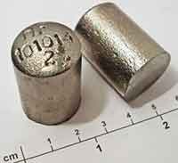 What is hafnium used for? This article aims to answer this question. Hafnium is a rare earth metal that has a high melting point and emission capacity. The metal can be used in many different applications. It is used in light bulbs, X-ray tubes, vacuum tubes, and rectifier elements. Hafnium is also used in plasma cutting electrodes. In addition, hafnium is used in a variety of chemical reactions, including catalysis and biotechnology.
Besides nuclear applications, hafnium is used in gas lamps, incandescent lamps, and in the construction of microchips. The metal is used in a variety of other applications, mainly in the nuclear industry. Hafnium can be used in refractory ceramic materials, microchips, and nozzles for plasma arc cutting. France is the largest producer of hafnium, producing 30 tons per year. However, 71% of the European Union depends on hafnium imports from China and Canada.
Hafnium is a silvery gray metal that is found in many minerals. It is most commonly found in conjunction with zirconium, and is difficult to separate. Hafnium is a nonreactive metal, meaning that it is unaffected by water, air, and most acids. Hafnium is used in high-temperature alloys and as a scavenger metal against oxygen. Its toxicity is unknown, but it is a dangerous element to work with.
Hafnium is extracted from zirconium by using an ion-exchange method. After separating the hafnium from the zirconium, the hafnium is formed as a pure metal. This material is known as hafnium tetra-iodide. In 1925, hafnium tetra-iodide was first made as a pure metal.
Video: What is Hafnium (HfO2)?
Important Terms for Electron Beam Evaporation
- Thermal evaporation
- Vacuum vaporization
- Vvaporization systems
- Vapor deposition
- Beam vaporization
- Vaporization device
- Reactive evaporation
- Evaporation beam
- Evaporation rates
- Vaporized material
- Vapour deposition
- Deposition technology
- Thermal barriers
- Beam evaporation
- Deposition deflection
What is Electron Beam Evaporation (E-Beam)?
If you're looking for an answer to the question "What is Electron Beam Evaporation?" then you've come to 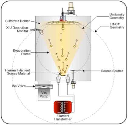 the right place. Here, you'll learn about the benefits and applications of this process and how much it costs. The next section will discuss the different types of evaporation materials used in the process. After that, you'll be ready to get started with your project!
Electron beam vaporation, or e-beam vaporation, is a type of Physical Vapor Deposition (PVD) technology that directly heats evaporating material, typically pellets, using an electron beam in a vacuum, and transfers the vaporized material onto the substrate to form a film. Electron Beam Sources for Electron Beam Deposition E-beam deposition is the technique of using electron beams generated from an electron source under vacuum to irradiate the vaporizing material, and heat and vaporize it, such that the vaporized material forms a thin film over the substance, such as the substrate or the objective. Common types of physical vapor deposition include vapor deposition and sputtering deposition. As mentioned earlier, there are two types of physical deposition techniques (sputtering and evaporation).
Is E-Gun the Same as Electron Beam Evaporation?
Electron beam evaporation is the same as E-Gun. The process of e-beam evaporation involves the use of a high-velocity electron beam accelerated to a high kinetic energy. These electrons quickly lose their energy when they strike the material. This kinetic energy is converted into thermal energy when the electrons strike the substrate. When the temperature of the evaporation material is high enough, the material will either melt or sublimate. In some cases, a solid film may result. Either way, a vapor is produced, which is then applied to a surface for coating.
Electron beam evaporation deposition can be used to deposit multiple materials from a single source. The target material is held at a positive potential relative to the filament. An additional electric field steers the beam over the surface of the ingot. Once the desired layer is formed, the process is repeated. This process can also be used to deposit multiple materials simultaneously on the same substrate. Electron beam evaporation is highly reliable and has been widely adopted for a number of applications.
Another use of e-beam evaporation is in the manufacturing of high-performance aerospace and automotive components. Electron beam evaporation creates materials with very high temperature and wear resistance, and it can be used to coat the inside surfaces of complex geometries. Electron beam evaporation is a very fast and efficient process, and it can also create optical films. Electron beam evaporation is used to produce conductive films in high-tech applications, including solar panels and architectural glass.
Another advantage of e-beam evaporation is its ability to produce good film stoichiometry. It is compatible with both ion assist sources and non-refractory materials. Electron beam evaporation has a wide range of applications, from metal deposition to dielectric coatings. Its advantages also include its low costs and compatibility with ion-assist sources.
Electron beam evaporation is the most efficient form of physical vapour deposition. Electron beams directly heat the evaporating material and transfer the vaporized material to the substrate. The resulting thin film has the greatest temperature in contact with the substrate. The HEX Series equipment by Korvus Technology is designed to achieve these high-quality results. If you're looking for a quality machine, it's worth investing in a high-end electron beam evaporator.
Electron beam evaporation is a form of physical vapor deposition that utilizes an intense electron beam generated from a tungsten filament. This beam has a high electricity density and enables efficient evaporation of materials with high melting points. Electron beam evaporation is especially effective for depositing high-melting-point metals and other high-temperature materials. It also allows for high-quality film coatings and is highly efficient in material utilization and reduces heat damage.
The EB-PVD process has been used to coat the surfaces of HPHT turbine components. It produces columnar microstructures and is very effective at strain-tolerant materials. Its evaporation rate can reach one millimeter per second. The EB-PVD process is one of the most common ways to coat a surface. However, it is not an ideal method for coating the inside of complex geometries.
What are E-Gun Applications?
E-gun evaporation deposition is a process that uses a high-voltage electron beam to deposit materials. The focused beam of electrons has a high density of electricity, allowing high-melting-point materials, such as silicon dioxide, to be efficiently deposited onto a substrate. These materials include platinum, silicon dioxide, and gold. Electron beam evaporators are also capable of depositing multiple layers in a single process.
Electron-beam evaporation devices consist of two main parts: an electron source that generates and accelerates electrons, and an evaporation material that absorbs the energy from the beam. Both sections can be used in tandem. The electron beam is heated directly by the high-voltage energy of the electrons, which is transferred into the evaporant material. EB-guns typically operate at a voltage of three to 40 kV.
Electron beam evaporation can be used to deposit low-resistance materials, including plastics, glass, and metals. It is more effective than resistance heating, making it an excellent method for creating wear-resistant coatings and components for the aerospace and automotive industries. Electron-beam evaporation can also produce multilayer optical thin films, which are required for architectural glass and other applications.
High energy evaporation can deposit thin films with a high density and improved adhesion to the substrate. Similarly, multiple crucible E-beam guns allow for the deposition of multiple layers of materials without interlayer contamination. A number of source materials, such as gold, platinum, and aluminum, have been deposited using this method. As the technology continues to evolve, more applications of e-gun evaporation deposition become possible.
Electron-beam evaporation uses a focused beam of electrons. Electrons typically have a temperature of 3000 degC. A 100 kV DC voltage source accelerates electrons toward their target. This method is especially useful for depositing metals with a high melting point. In addition, evaporation takes place in a localized point near the source of bombardment. This process also eliminates the contamination from the crucible. Electrons lose energy rapidly, transforming kinetic energy into thermal energy.
Electron beam evaporation uses a high-voltage electron beam generated from a filament. The beam is steered by electric and magnetic fields to vaporize a source material. This deposition technique is capable of coating a substrate above the evaporating material. The distances between the source and substrate are 300mm to one meter. This process is often used to coat a substrate.
Electron-beam evaporation is used for deposition of high-melting-point materials and dielectrics. It is a versatile process that is compatible with ion-assist sources. The high-efficiency and uniformity of e-beam evaporation enable it to be used for a number of different applications. When used properly, it is possible to achieve multiple layers in one deposition process.
What Does E-Gun Evaporation Cost?
The cost of E-gun evaporation deposition systems varies, depending on the system's capabilities. The E-gun evaporator contains a single mass spectrometer, which switches every 16 ms between the two evaporated materials. The system includes liquid nitrogen panels, a titanium sublimator, a turbo molecular pump, and sample holders. The rate control system also includes an ionization chamber, a radio frequency generator, and a QMG511 mass spectrometer.
The evaporation chamber for the EBVD system is a high-vacuum chamber and can support up to eight materials at once. The chamber can be operated at 5.0x10⁻³ Torr, and multiple types of evaporation materials can be deposited in the same process. There are several methods of generating electron beams, including thermionic emission and field electron emission. Another method is the anodic arc method.
Rate-controlled e-guns are also possible with feedback applied to many materials. The accuracy of rate control depends on the sensor's sensitivity and bandwidth. High-frequency evaporation sensors such as mass spectrometers are suitable for rate control because of their high sensitivity and wide bandwidth. Improved e-gun design and improved power supply can improve rate stability. The objective is a more stable beam profile and less evaporation noise.
While an E-gun can be used for deposition of multiple materials, a higher rate of deposition is more expensive. Deposition rates of one material at a time will be significantly higher than other materials. Evaporation rates must be high enough to meet a substrate's requirements. In general, an E-gun deposition process requires more than a single gun, and two separate guns may be necessary.
A traditional electronic-gun can be controlled by an I-controller. The e-gun is a Temescal SFIH-270-2. The output is shown in figure 7. A higher gain A increases the noise suppression. Likewise, an increase in gain B will make the deposition rate more stable. Using a high-frequency control e-gun can increase rate stability. E-guns with a wehnelt electrode, for example, can control evaporation rates at 140 Hz.
The E-gun is another method for reducing the noise associated with evaporation. A sweeping motion of the spot over the melt can also reduce noise. This sweeping motion can also help reduce the partial pressure of the melt above it. The frequency of the sweep should be higher than the response time of the melt to avoid excessive noise. This method is also effective in coating the inner surface of complex geometries.
Silicon and E-Beam Evaportion Steps
Here's a detailed guide on how to use silicon substrates with electron beam evaporation, along with images and a flow chart.
Guide to Using Silicon Substrates with Electron Beam Evaporation
Step 1: Preparation of Silicon Substrates
- Clean the silicon substrates thoroughly to remove any contaminants.
- Use a standard cleaning procedure like RCA clean.
- Dry the substrates using nitrogen gas.
![]()
Step 3: Setting Up the Electron Beam Evaporator
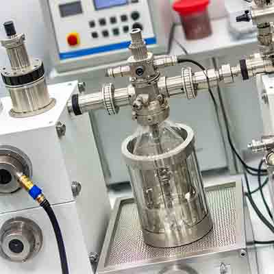
- Place the material to be evaporated in the crucible of the electron beam evaporator.
- Ensure the vacuum chamber is sealed properly.
- Evacuate the chamber to achieve a high vacuum (around 10−6−10−710^{-6} - 10^{-7} Torr).
Step 4: Evaporation Process
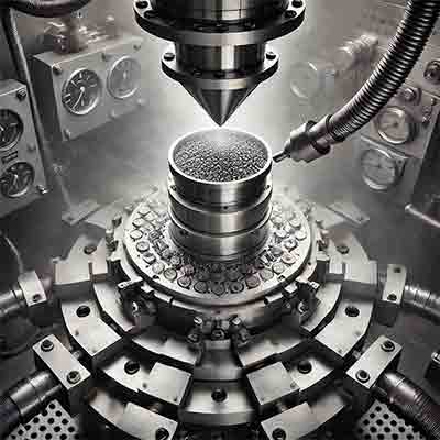
- Heat the material using the electron beam until it starts to evaporate.
- Monitor the deposition rate and thickness using a quartz crystal microbalance.
- Rotate the substrate holder for uniform coating.
Step 5: Cooling and Unloading
- Once the desired thickness is achieved, turn off the electron beam and allow the system to cool.
- Vent the vacuum chamber slowly to avoid introducing contaminants.
- Unload the coated silicon substrates carefully.

Step 6: Post-Deposition Treatment
- Inspect the coated substrates using techniques like scanning electron microscopy (SEM) or atomic force microscopy (AFM).
- Perform any necessary annealing or further processing as required.
Flow Chart
Start
- Clean Silicon Substrates
- Dry with Nitrogen Gas
- Load into Substrate Holder
- Set Up Electron Beam Evaporator
- Place Material in Crucible
- Evacuate Vacuum Chamber
- Heat Material with Electron Beam
- Monitor Deposition Rate and Thickness
- Rotate Substrate Holder for Uniform Coating
- Turn Off Electron Beam and Cool
- Vent Vacuum Chamber
- Unload Coated Silicon Substrates
- Inspect and Post-Process Substrates
End
