
We are developing fully depleted SOI transistors for low-power integrated circuit research and require an SOI substrate with a thin silicon device layer and controlled buried oxide thickness. We need material suitable for CMOS-compatible processing and would like to know whether SIMOX or another SOI structure is available for our required specifications.
SIMOX Wafers for Semiconductor Research
SIMOX (Separation by IMplanted OXygen) is a method used to form silicon-on-insulator (SOI) material by implanting a high dose of oxygen ions into a silicon wafer and subsequently performing high-temperature annealing. The process produces a buried oxide (BOX) layer beneath a crystalline silicon device layer.
This silicon / buried oxide / silicon structure provides electrical isolation between the active device layer and the underlying substrate. Depending on the device design, SOI isolation can help reduce junction capacitance and substrate coupling compared with conventional bulk-silicon structures.
SIMOX substrates have therefore been investigated and used for applications including SOI electronics, RF devices, radiation-tolerant electronics, MEMS, sensors, and specialized semiconductor research.
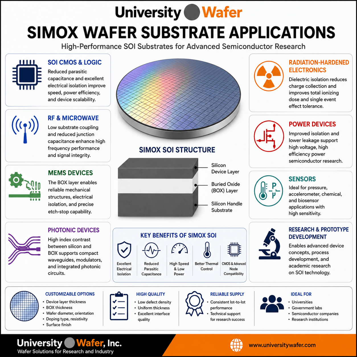
SIMOX Wafer Structure
A typical SIMOX substrate contains three principal regions:
- Silicon device layer – the upper crystalline silicon region in which semiconductor devices or microstructures can be fabricated.
- Buried oxide (BOX) – an electrically insulating SiO2 layer formed below the surface through oxygen implantation and subsequent annealing.
- Silicon handle substrate – the underlying silicon wafer that provides mechanical support.
The thickness and quality of these layers are important because they can influence electrical isolation, electrostatic behavior, thermal transport, mechanical properties, and device processing.
How SIMOX Wafers Are Made
SIMOX fabrication begins with a high-quality single-crystal silicon wafer . Oxygen ions are implanted below the wafer surface at energies and doses selected to establish the desired oxygen-rich region.
The implanted wafer is then subjected to high-temperature annealing. During this thermal treatment, the implanted oxygen forms a buried silicon dioxide region while the damaged silicon above the implanted region undergoes substantial crystalline recovery.
The resulting material is an SOI structure with a silicon device layer separated from the bulk silicon substrate by the BOX layer. Actual layer thicknesses, defect densities, interface characteristics, and uniformity depend on the specific SIMOX process conditions.
Why Researchers Use SIMOX SOI Substrates
The buried oxide changes the electrical interaction between devices fabricated in the upper silicon layer and the underlying silicon substrate. This can provide several useful characteristics for semiconductor research.
- Electrical isolation – the BOX electrically separates the device layer from the silicon handle substrate.
- Reduced junction capacitance – appropriate SOI device structures can reduce parasitic junction capacitance relative to comparable bulk-silicon designs.
- Reduced substrate coupling – useful for selected RF and mixed-signal device architectures.
- Thin silicon device layers – enable research into thin-body SOI devices and specialized microelectronic structures.
- Radiation-tolerant architectures – dielectric isolation can provide advantages for certain radiation-effects and radiation-hardened device designs.
- Compatibility with silicon processing – the crystalline silicon surface can be processed using many established semiconductor fabrication techniques.
These advantages are device- and process-dependent, so researchers should evaluate the complete SOI structure rather than assuming that every SIMOX substrate provides the same electrical performance.
SIMOX Wafer Specifications to Consider
When requesting a SIMOX wafer, researchers should provide as much information as possible about the required substrate. Important specifications can include:
- Wafer diameter
- Silicon device-layer thickness
- Buried oxide (BOX) thickness
- Crystal orientation
- Conductivity type – p-type or n-type
- Resistivity or dopant requirements
- Surface finish
- Thickness uniformity requirements
- Defect or interface-quality requirements, when critical to the experiment
- Quantity
Device-layer and BOX thickness are especially important because they affect device electrostatics, isolation, capacitance, and thermal behavior.
SIMOX for Fully Depleted SOI Research
Thin silicon device layers are important in fully depleted SOI (FD-SOI) device research. When the silicon body is sufficiently thin and the device is appropriately designed, the semiconductor body can become fully depleted during operation, providing different electrostatic behavior from conventional bulk MOSFET structures.
However, suitability for a particular FD-SOI process depends on more than simply using an SOI or SIMOX substrate. Researchers may require tightly controlled silicon thickness, BOX thickness, thickness uniformity, crystal quality, interface quality, doping, and surface condition.
When requesting material for FD-SOI research, provide the target device-layer and BOX specifications so the available SOI options can be evaluated against the process requirements.
Common SIMOX Research Applications
SIMOX and related SOI structures have been studied for a range of semiconductor and microsystem applications, including:
- SOI CMOS research
- Thin-body and fully depleted transistor research
- RF and microwave electronics
- Radiation-effects and radiation-hardened electronics
- MEMS sensors and microstructures
- Mixed-signal and specialized integrated circuits
- Silicon device physics research
- Semiconductor process development
For applications such as photonics or MEMS, researchers should select the SOI architecture based on the required optical, mechanical, thermal, and dimensional properties rather than assuming SIMOX is preferable to other SOI fabrication methods.
SIMOX vs. Other SOI Wafer Technologies
SIMOX is one method of producing an SOI substrate. Other SOI technologies use wafer bonding, layer transfer, thinning, or combinations of these processes to create a silicon device layer above an insulating oxide.
The best SOI substrate for a research project depends on factors such as device-layer thickness, BOX thickness, crystalline quality, interface quality, wafer diameter, thermal requirements, defect tolerance, and device architecture.
Researchers should therefore compare the actual wafer specifications rather than treating SIMOX and bonded SOI as interchangeable materials.
Researcher SIMOX Wafer Request
For requests like this, include the required wafer diameter, device-layer thickness, BOX thickness, orientation, conductivity type, resistivity, surface finish, and quantity. Any critical requirements for interface quality, defect density, or thickness uniformity should also be specified.
Request SIMOX or SOI Wafers
UniversityWafer supplies SOI wafers and specialty silicon substrates for semiconductor research, device development, MEMS, microfabrication, and university laboratories. Availability of specific SIMOX structures depends on the required wafer and layer specifications.
Get Your SIMOX or SOI Wafer Quote FAST! Submit your specifications below or Buy Wafers Online.
How SIMOX Structure Affects Device Performance
A SIMOX silicon-on-insulator wafer contains a crystalline silicon device layer separated from the silicon handle substrate by a buried silicon dioxide (BOX) layer. This dielectric isolation changes how electrical signals, heat, and mechanical structures interact with the underlying substrate.
In appropriately designed devices, the BOX can reduce junction capacitance and substrate coupling compared with conventional bulk-silicon structures. These characteristics have made SIMOX and other SOI technologies useful for research involving CMOS, RF electronics, radiation effects, MEMS, sensors, and specialized integrated devices.
Device performance cannot be predicted from the presence of a BOX layer alone. Device-layer thickness, BOX thickness, interface quality, defect density, handle-wafer resistivity, doping, and fabrication conditions must all be considered.
SIMOX for RF and Microwave Research
Electrical isolation from the handle substrate can be advantageous in RF, microwave, analog, and mixed-signal circuits because substrate coupling and parasitic capacitance can affect high-frequency performance.
Researchers evaluating SIMOX or other SOI wafers for RF applications should consider:
- Handle-wafer resistivity
- BOX thickness and quality
- Device-layer thickness and resistivity
- Interface charge and trap density
- Parasitic conduction near the BOX/handle interface
- Operating frequency and device architecture
Potential research structures include RF switches, transmission lines, passive components, amplifiers, mixers, oscillators, and other integrated high-frequency devices.
Radiation Effects and SIMOX SOI
SIMOX has a long history in radiation-effects and radiation-hardened electronics research. Dielectric isolation can reduce some parasitic interactions with the bulk substrate, making SOI attractive for devices intended for radiation environments.
However, the buried oxide itself can respond to ionizing radiation. Radiation-induced charge trapping in the oxide and at interfaces can alter transistor characteristics, so SOI should not be assumed to be intrinsically immune to radiation damage.
Radiation performance depends on factors including BOX quality, transistor geometry, fabrication process, total ionizing dose, particle environment, bias conditions, and operating temperature.
SIMOX substrates can therefore be useful for research involving:
- Space and satellite electronics
- Radiation-response characterization
- Particle-detector electronics
- Nuclear instrumentation
- High-energy physics electronics
- Radiation-hardened integrated-circuit development
SIMOX Wafers for MEMS and Sensors
The silicon/BOX/silicon architecture can also be useful for MEMS fabrication. The crystalline device layer provides a structural material, while the BOX can provide electrical isolation and, in suitable fabrication sequences, function as an etch-stop or sacrificial oxide layer.
Device-layer thickness is especially important for MEMS because it can influence the dimensions, stiffness, mass, resonant frequency, and mechanical behavior of fabricated structures.
Potential research applications include:
- Pressure sensors
- Accelerometers and inertial sensors
- MEMS resonators
- Microheaters
- Mechanical test structures
- Microfluidic and microsystem research
- Integrated electrical and optical sensors
SIMOX and Silicon Photonics Research
SOI substrates are widely used in silicon photonics because crystalline silicon has a substantially higher refractive index than silicon dioxide. The resulting index contrast can provide strong optical confinement in appropriately designed silicon waveguides.
SIMOX material may be evaluated for photonics research, but suitability depends on optical requirements and material quality. Important parameters can include:
- Silicon device-layer thickness
- Buried oxide thickness
- Device-layer thickness uniformity
- Surface and interface roughness
- Optical loss and absorption
- Defects and contamination
Research structures can include silicon waveguides, optical resonators, modulators, photonic sensors, and integrated optical circuits. For demanding photonics applications, researchers should compare the actual SIMOX material specifications with those of other SOI technologies before selecting the substrate.
Thermal Considerations for SIMOX Devices
The buried oxide provides valuable electrical isolation, but it also changes the thermal behavior of the device. Silicon dioxide has substantially lower thermal conductivity than crystalline silicon, so the BOX can impede heat flow from the active silicon layer into the handle substrate.
This can contribute to self-heating in devices with significant power dissipation. Thermal effects should therefore be considered when using SIMOX or other SOI substrates for high-current, high-power, or densely integrated devices.
Relevant design parameters include device geometry, silicon thickness, BOX thickness, operating power, thermal contacts, backside processing, and packaging.
SIMOX Material Quality and Defects
SIMOX formation requires energetic oxygen implantation followed by high-temperature annealing. Because ion implantation initially damages the silicon lattice, the final material quality depends strongly on implantation and annealing conditions.
Depending on the SIMOX process, researchers may need to consider defects or nonuniformities involving the silicon device layer, BOX, and their interfaces. For demanding experiments, material characterization may therefore be as important as nominal device-layer and BOX thickness.
Relevant quality parameters can include:
- Device-layer crystalline quality
- BOX continuity and uniformity
- Silicon/oxide interface quality
- Surface roughness
- Dislocations and stacking faults
- Particles and surface defects
- Thickness uniformity
- Electrical defect density
Characterizing SIMOX Wafers
Characterization methods should be selected according to the device requirements and the properties that need to be verified. Common techniques can include:
| Technique | What It Can Evaluate |
|---|---|
| Ellipsometry | Silicon and oxide layer thicknesses and optical properties |
| Four-Point Probe | Sheet resistance and electrical uniformity of suitable conductive layers |
| AFM | Surface topography and roughness |
| SIMS | Depth profiles of oxygen, dopants, and selected impurities |
| TEM | Layer structure, interfaces, crystalline defects, and BOX morphology |
| Optical / Defect Inspection | Particles, surface imperfections, and selected wafer defects |
| Bow / Warp / TTV Measurement | Wafer geometry and dimensional uniformity |
Processing SIMOX SOI Wafers
The upper layer is crystalline silicon, so many established microfabrication processes can be applied to SIMOX substrates. However, recipes developed for bulk silicon may require adjustment because of the thin device layer and buried oxide.
- Account for the device-layer thickness when selecting implantation or diffusion conditions.
- Consider silicon-to-SiO2 etch selectivity when using the BOX as an etch stop.
- Evaluate thermal budgets when subsequent high-temperature processing is required.
- Consider BOX-related self-heating for devices with substantial power dissipation.
- Verify backside and wafer-bonding requirements before selecting handle-wafer thickness.
- Use clean semiconductor handling and storage procedures to minimize surface contamination and particles.
SIMOX vs. Bonded SOI: Which Should You Choose?
SIMOX and bonded SOI can produce the same basic architecture—a silicon device layer above a buried oxide—but their manufacturing methods and resulting material characteristics can differ.
| Consideration | SIMOX | Bonded / Layer-Transfer SOI |
|---|---|---|
| SOI Formation | High-dose oxygen implantation followed by annealing | Wafer bonding combined with thinning or layer transfer |
| Buried Oxide | Formed inside the implanted silicon wafer | Typically associated with an oxidized surface incorporated during bonding |
| Key Material Concern | Implantation-related defects and BOX/interface quality | Bond/interface quality, transferred-layer quality, and thickness uniformity |
| Selection Basis | Device-layer thickness, BOX thickness, crystal quality, interfaces, resistivity, thermal requirements, wafer size, availability, and device architecture | |
Neither technology is universally superior. Researchers should select the SOI material whose measured and specified properties best match the intended fabrication process and device.
Related SIMOX, SOI and Semiconductor Resources
- Silicon-on-Insulator (SOI) Wafers – Explore SOI substrates, device-layer and buried oxide specifications, and research applications.
- Silicon Wafers – Explore silicon substrates by diameter, orientation, resistivity, dopant type, thickness, and surface finish.
- Silicon Epitaxy – Learn about epitaxial silicon layers and their use in advanced semiconductor device structures.
- Microfabrication – Explore lithography, etching, deposition, oxidation, and other processes used to fabricate devices on semiconductor wafers.
- MEMS Fabrication – Learn how silicon and SOI substrates are used to fabricate sensors, resonators, actuators, and microsystems.
- Silicon Wafer Doping Techniques – Compare methods used to control carrier concentration and electrical resistivity in silicon.
- Thermal Oxide on Silicon – Learn how SiO2 layers are formed on silicon and used for electrical isolation, masking, and semiconductor processing.
- Silicon Wafer Applications – Explore applications in integrated circuits, MEMS, sensors, photonics, photovoltaics, and semiconductor research.
- Photolithography – Learn how patterns are transferred onto silicon and SOI substrates during microdevice fabrication.
- Silicon Wafer Orientation – Compare (100), (110), and (111) silicon orientations and their importance in semiconductor processing.